Äîêóìåíòàöèÿ è îïèñàíèÿ www.docs.chipfind.ru
SCHOTTKY RECTIFIER
3.0 Amp
MBRD320
MBRD330
MBRD340
Bulletin PD-20756 rev. D 03/03
1
www.irf.com
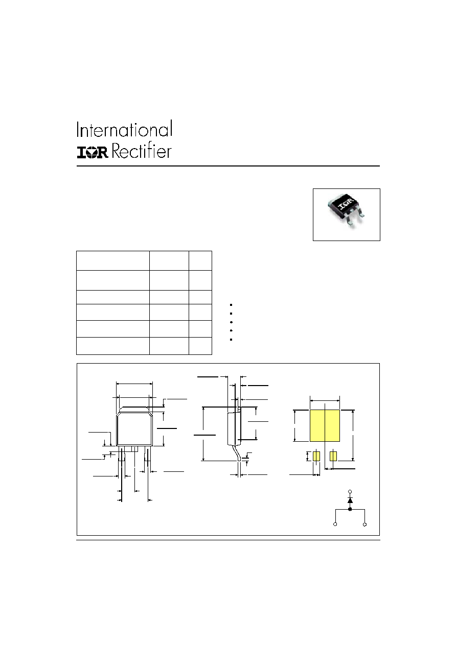
Major Ratings and Characteristics
I
F(AV)
Rectangular
3.0
A
waveform
V
RRM
20 - 30 - 40
V
I
FSM
@ tp = 5 µs sine
490
A
V
F
@
3 Apk, T
J
= 125°C
0.49
V
T
J
- 40 to 150
°C
Characteristics
Value
Units
Description/ Features
The MBRD320, MBRD330, MBRD340 surface mount
Schottky rectifier has been designed for applications requiring
low forward drop and small foot prints on PC board. Typical
applications are in disk drives, switching power supplies,
converters, free-wheeling diodes, battery charging, and
reverse battery protection.
Popular D-PAK outline
Small foot print, surface mountable
Low forward voltage drop
High frequency operation
Guard ring for enhanced ruggedness and long term
reliability
6.73 (0.26)
6.35 (0.25)
5.46 (0.21)
5.21 (0.20)
4
1.27 (0.05)
0.88 (0.03)
5.97 (0.23)
1 - Anode
2 - Cathode
3 - Anode
4 - Cathode
1.64 (0.02)
1.52 (0.06)
1.15 (0.04)
1.14 (0.04)
0.76 (0.03)
2x
2.28 (0.09)
2x
0.89 (0.03)
0.64 (0.02)
3x
4.57 (0.18)
1
2
3
6.22 (0.24)
2.38 (0.09)
2.19 (0.08)
6.45 (0.24)
5.68 (0.22)
10.42 (0.41)
9.40 (0.37)
0.46 (0.02)
0.58 (0.02)
1.14 (0.04)
0.89 (0.03)
0.51 (0.02)
MIN.
0.58 (0.02)
0.46 (0.02)
MINIMUM RECOMMENDED FOOTPRINT
5.97 (0.24)
10.67 (0.42)
1.65 (0.06)
6.48 (0.26)
2x
2.54 (0.10)
2x
2.28 (0.09)
2x
Dimensions in millimeters and (inches)
Conform to JEDEC outline D-Pak (Similar to TO-252AA)
D-Pak (TO-252AA)
Anode
1
3
Base
Cathode
Anode
4, 2
MBRD320, MBRD330, MBRD340
Bulletin PD-20756 rev. D 03/03
2
www.irf.com
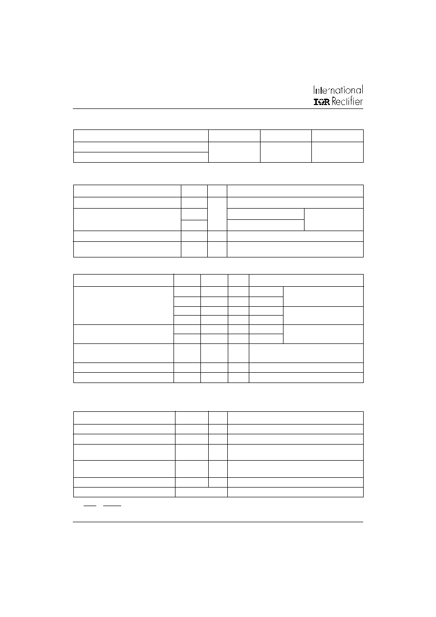
Part number
MBRD320
MBRD330
MBRD340
V
R
Max. DC Reverse Voltage (V)
20
30
40
V
RWM
Max. Working Peak Reverse Voltage (V)
Voltage Ratings
T
J
Max. Junction Temperature Range
(*)
- 40 to 150
°C
T
stg
Max. Storage Temperature Range
- 40 to 175
°C
R
thJC
Max. Thermal Resistance Junction
6.0
°C/W DC operation * See Fig. 4
to Case
R
thJA
Max. Thermal Resistance Junction
80
°C/W
to Ambient
wt
Approximate Weight
0.3 (0.01)
g (oz.)
Case Style
D - PAK
Similar to TO-252AA
Thermal-Mechanical Specifications
Parameters
Value
Units
Conditions
V
FM
Max. Forward Voltage Drop (1)
0.48
0.6
V
@ 3A
See Fig. 1
0.58
0.7
V
@ 6A
0.41
0.49
V
@ 3A
0.55
0.625
V
@ 6A
I
RM
Max. Reverse Leakage Current (1)
0.02
0.2
mA
T
J
= 25 °C
See Fig. 2
10.7
20
mA
T
J
= 125 °C
C
T
Typical Junction Capacitance
189
-
pF
V
R
= 5V
DC
(test signal range 100kHz to
1Mhz), @ 25°C
L
S
Typical Series Inductance
5.0
-
nH
Measured lead to lead 5mm from package body
dv/dt Max. Voltage Rate of Change
-
10000
V/ µs
(Rated V
R
)
(1) Pulse Width < 300µs, Duty Cycle <2%
T
J
= 25 °C
Electrical Specifications
Parameters
Typ.
Max.
Units Conditions
V
R
= rated V
R
T
J
= 125 °C
<
thermal runaway condition for a diode on its own heatsink
(*) dPtot
1
dTj
Rth( j-a)
I
F(AV)
Max. Average Forward Current
3.0
A
50% duty cycle @ T
L
= 133°C, rectangular wave form
I
FSM
Max. Peak One Cycle Non-Repetitive
490
5µs Sine or 3µs Rect. pulse
Surge Current
75
10ms Sine or 6ms Rect. pulse
E
AS
Non Repetitive Avalanche Energy
8.0
mJ
T
J
= 25 °C, I
AS
= 1Amp, L = 16mH
I
AR
Repetitive Avalanche Current
1.0
A
Current decaying linearly to zero in 1 µsec
Frequency limited by T
J
max. Va = 1.5 x Vr typical
Parameters
Value Units Conditions
Absolute Maximum Ratings
Following any rated
load condition and
with rated V
RRM
applied
MBRD320, MBRD330, MBRD340
Bulletin PD-20756 rev. D 03/03
3
www.irf.com
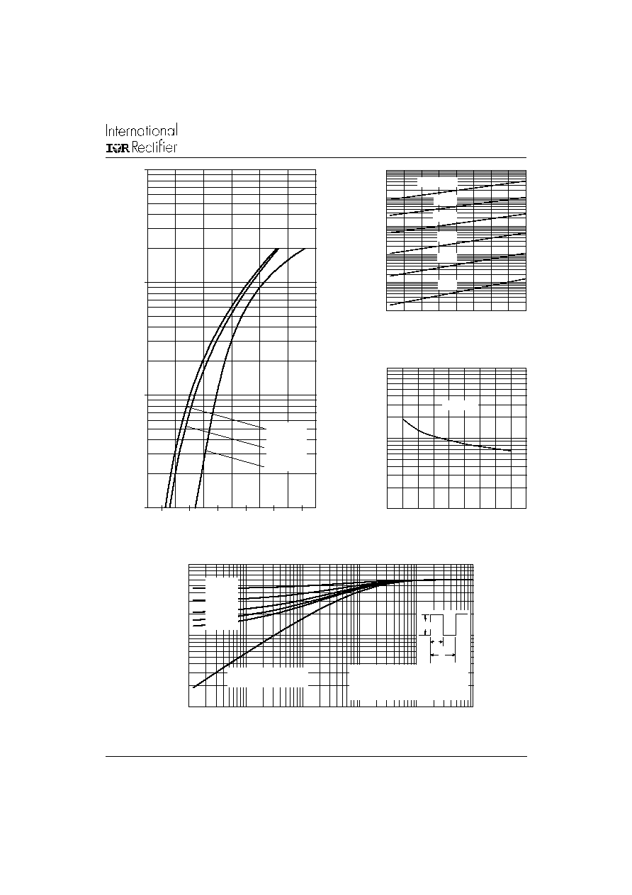
Fig. 2 - Typical Values of Reverse Current
Vs. Reverse Voltage
Fig. 3 - Typical Junction Capacitance
Vs. Reverse Voltage
Fig. 4 - Maximum Thermal Impedance Z
thJC
Characteristics
Fig. 1 - Maximum Forward Voltage Drop Characteristics
Forward Voltage Drop - V
FM
(V)
Instantaneous Forward Current - I
F
(A)
t
1
, Rectangular Pulse Duration (Seconds)
Thermal Impedance - Z
thJC
(°C/W)
Reverse Current (mA)
Reverse Voltage - V
R
(V)
0.001
0.01
0.1
1
10
100
0
5
10
15
20
25
30
35
40
125°C
100°C
75°C
50°C
25°C
Tj = 150°C
Reverse Voltage - V
R
(V)
Junction Capacitance C
T
(pF)
10
100
1000
0
5
10 15 20 25 30 35 40 45
Tj = 25°C
0.1
1
10
100
0
0.2
0.4
0.6
0.8
1
1.2
Tj = 150°C
Tj = 125°C
Tj = 25°C
0.1
1
10
0.00001
0.0001
0.001
0.01
0.1
1
Single Pulse
(Thermal Resistance)
D = 0.75
D = 0.50
D = 0.33
D = 0.25
D = 0.20
Notes:
1. Duty factor D = t1/ t2
2. Peak Tj = Pdm x Z thJC + Tc
2
t
1
t
P
DM
MBRD320, MBRD330, MBRD340
Bulletin PD-20756 rev. D 03/03
4
www.irf.com
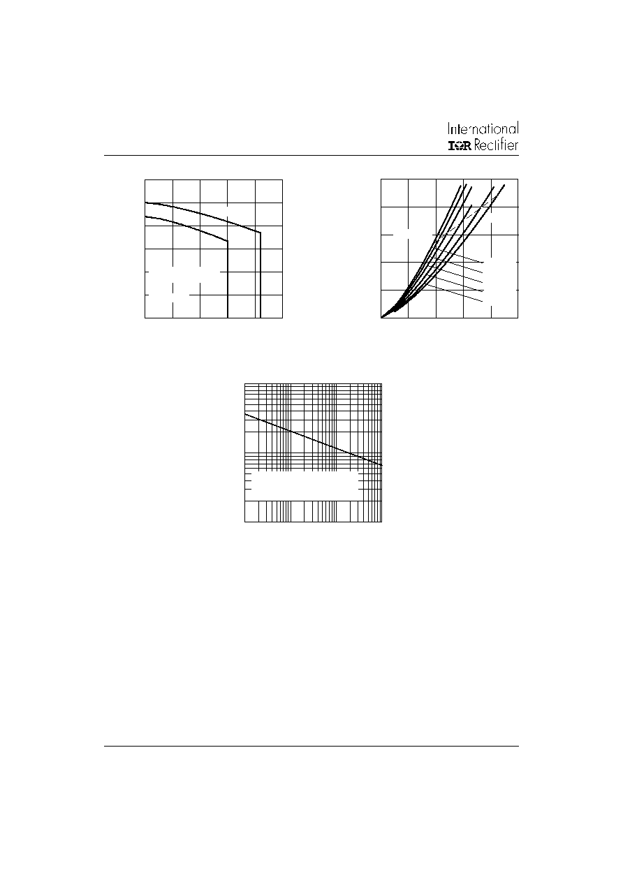
Fig. 5 - Maximum Allowable Case Temperature
Vs. Average Forward Current
Fig. 6 - Forward Power Loss Characteristics
Fig. 7 - Maximum Non-Repetitive Surge Current
(2) Formula used: T
C
= T
J
- (Pd + Pd
REV
) x R
thJC
;
Pd = Forward Power Loss = I
F(AV)
x V
FM
@ (I
F(AV)
/
D) (see Fig. 6);
Pd
REV
= Inverse Power Loss = V
R1
x I
R
(1 - D); I
R
@ V
R1
= 80% rated V
R
Average Forward Current - I
F(AV)
(A)
Allowable Case Temperature (°C)
Average Power Loss (Watts)
Average Forward Current - I
F(AV)
(A)
Square Wave Pulse Duration - t
p
(microsec)
Non-Repetitive Surge Current - I
FSM
(A)
100
110
120
130
140
150
160
0
1
2
3
4
5
DC
Square wave (D = 0.50)
80% Rated Vr applied
see note (2)
0
0.5
1
1.5
2
2.5
0
1
2
3
4
5
DC
RMS Limit
D = 0.20
D = 0.25
D = 0.33
D = 0.50
D = 0.75
10
100
1000
10
100
1000
10000
At Any Rated Load Condition
And With rated Vrrm Applied
Following Surge
MBRD320, MBRD330, MBRD340
Bulletin PD-20756 rev. D 03/03
5
www.irf.com
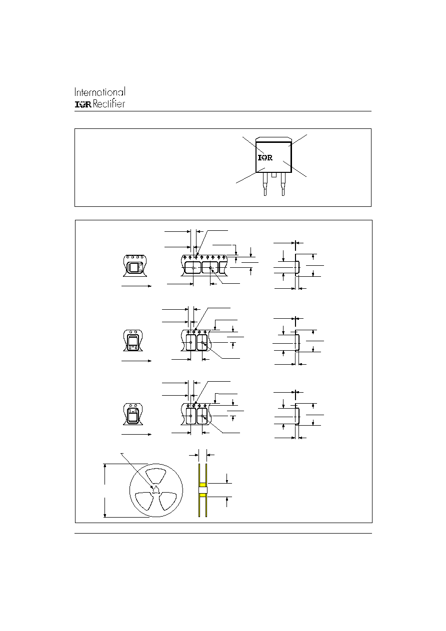
Tape & Reel Information
TR
FEED DIRECTION
4.1 (0.16)
3.9 (0.15)
2.1 (0.83)
1.9 (0.07)
12.1 (0.48)
1.65 (0.06)
1.85 (0.07)
1.65 (0.06)
7.4 (0.29)
2.6 (0.10)
1.5 (0.06)
7.6 (0.30)
11.9 (0.47)
1.85 (0.07)
TO-252AA Tape & Reel
When ordering, indicate the part
number, part orientation, and the
quantity. Quantities are in multiples
of 2,000 pieces per reel for TR and
multiples of 3,000 pieces per reel
for both TRL and TRR.
13 (0.52) DIA.
DIA. MAX.
375 (14.17)
50 (1.97) DIA.
22.4 (0.88)
0.35 (0.01)
16.3 (0.64)
15.7 (0.62)
2.75 (0.11)
2.55 (0.10)
0.25 (0.01)
6.8 (0.26)
7.0 (0.28)
TRR
FEED DIRECTION
4.1 (0.16)
3.9 (0.15)
2.1 (0.83)
1.9 (0.07)
8.1 (0.32)
1.85 (0.07)
1.65 (0.06)
1.85 (0.07)
1.65 (0.06)
7.4 (0.29)
2.6 (0.10)
1.5 (0.06)
7.6 (0.30)
7.9 (0.31)
0.35 (0.01)
16.3 (0.64)
15.7 (0.62)
2.75 (0.11)
2.55 (0.10)
0.25 (0.01)
10.4 (0.41)
10.6 (0.42)
DIA.
TRL
FEED DIRECTION
4.1 (0.16)
3.9 (0.15)
2.1 (0.83)
1.9 (0.07)
8.1 (0.32)
1.85 (0.07)
1.65 (0.06)
1.85 (0.07)
1.65 (0.06)
7.4 (0.29)
2.6 (0.10)
1.5 (0.06)
7.6 (0.30)
7.9 (0.31)
0.35 (0.01)
16.3 (0.64)
15.7 (0.62)
2.75 (0.11)
2.55 (0.10)
0.25 (0.01)
10.4 (0.41)
10.6 (0.42)
DIA.
DIA.
DIA.
DIA.
DIA.
Marking Information
EXAMPLE: THIS IS A MBRD340
5K3A
MBRD340
712A
INTERNATIONAL
RECTIFIER LOGO
PART NUMBER
ASSEMBLY
LOT CODE
4 (K)
1 (A)
3 (A)
2 (K)
DATE CODE (YWWA)
Y
= YEAR
WW = WEEK
A
= LINE