H-SERIES-TRIPLE.pmd
07/16/02
www.irf.com
1
ADVANCED ANALOG
HIGH RELIABILITY RADIATION
HARDENED DC/DC CONVERTERS
H-SERIES
Description
n
Total Dose > 25K Rad(Si)
n
SEE > 37 MeV
.
cm
2
/mg
n
Internal EMI filter; Converter Capable of
meeting MIL-STD-461C CE03 and CS01
n
Low Weight, < 125 grams
n
Magnetically Coupled Feedback
n
18V to 50V Input Range ( 50V, 70V, and
120V Models Available)
n
Up to 40W Output Power
n
Triple Output Models Include
+5 and
±
12 or
±
15V
n
Main output isolated from dual outputs
n
High Efficiency - to 80%
n
-55°C to +125°C Operating Temperature
Range
n
100M
@ 500VDC Isolation
n
Under-Voltage Lockout
n
Short Circuit and Overload Protection
n
Output Over Voltage Limiter
n
External Inhibit
n
> 1,500,000 Hour MTBF
Features
+28V Input, Triple Output
The H-Series of DC/DC converters are radiation toler-
ant, high reliability devices designed for moderate ra-
diation environments such as those encountered by low
earth orbit satellites and launch vehicles. For higher
radiation environments, the G-Series of DC/DC con-
verters is recommended. System upgrades to higher
radiation tolerance applications can be easily accom-
modated with the G-Series converters because they
have the same mechanical outline and are pin compat-
ible. For physically smaller, lower output power single
and dual output applications the L-Series of DC/DC con-
verters are recommended. Features of the H-Series in-
clude up to 40 watt output power, small size, low weight
and a high tolerance to total ionizing dose, single event
effects and environmental stresses such as tempera-
ture extremes, mechanical shock, and vibration. All com-
ponents are fully derated to meet the requirements of
MIL-STD-975 and MIL-STD-1547. Extensive documen-
tation including Radiation Susceptibility, Thermal Analy-
sis, Stress Analysis and MTBF are available.
The converters incorporate a fixed frequency single for-
ward topology with magnetic feedback and an internal
EMI filter. These converters are capable of meeting the
conducted emissions and conducted susceptibility re-
quirements of MIL-STD-461C without any additional
components. All models include an external inhibit port
and have an adjustable output voltage. They are en-
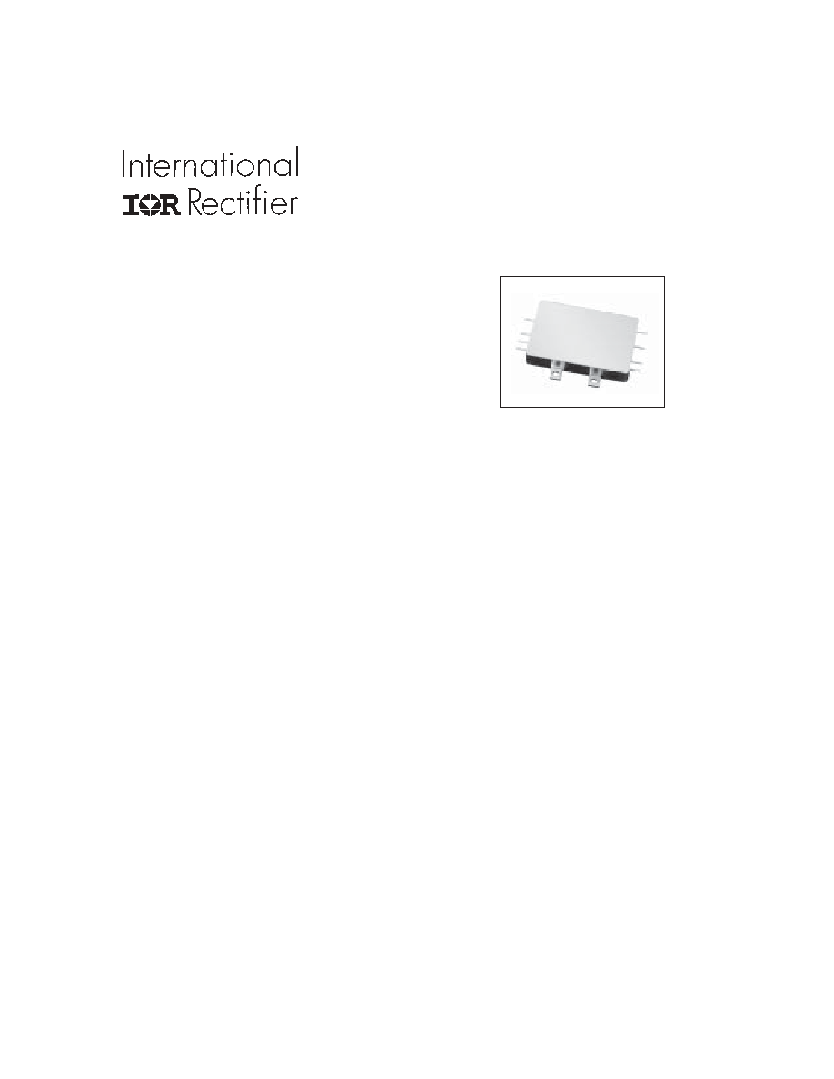
closed in a hermetic 3.0" x 2.5" x 0.445" steel package
and weigh less than 125 grams. The package utilizes
rugged ceramic feed-through copper core pins and is
sealed using parallel seam welding.
Full environmental screening includes temperature cy-
cling, constant acceleration, fine and gross leak, and
burn-in.
electrical specifications and screening to meet
custom requirements can be accommodated.
Applications
n
Low Earth Orbit Satellites (LEO)
n
Launch Vehicles
Non-flight versions of the H-Series converters are avail-
able for system development purposes. Variations in
PD - 94518

2
www.irf.com
H-SERIES
The H-Series converters utilize a single forward to-
pology with resonant reset. The nominal switching
frequency is 500kHz. Electrical isolation and tight
output regulation are achieved through the use of a
magnetically coupled feedback. Voltage feed-forward
with duty factor limiting provides high line rejection
and protection against output over voltage in the
event of an internal control loop failure. This mecha-
nism limits the maximum output voltage to approxi-
mately 20% over the nominal regardless of the line
voltage.
Circuit Description
An internal EMI filter allows the converter to meet the
conducted emissions requirements of MIL-STD-461C
on the input power leads. A two-stage output filter
reduces the typical output ripple to less than 20mV
peak-to-peak.
An under-voltage lockout circuit prohibits the con-
verter from operating when the line voltage is too
low to maintain the output voltage. The converter will
not start until the line voltage rises to approximately
17 volts and will shut down when the input voltage
drops below 16 volts. The one volt of hysteresis re-
duces the possibility of line noise interfering with the
converter's start-up and shut down.
An external inhibit port is provided to control con-
verter operation. The converter's operation is inhib-
ited when this pin is pulled low. It is intended to be
driven by an open collector logic device. The pin
may be left open for normal operation and has a
nominal open circuit voltage of 10.5V with respect to
the input return (pin 2).
Design Methodology
The H-Series was developed using a proven con-
servative design methodology which includes se-
lecting radiation tolerant and established reliability
components and fully derating to the requirements
of MIL-STD-975 and MIL-STD-1547. Heavy derat-
ing of the power MOSFET gate and drain voltages
minimize the possibility of SEGR and SEB. A mag-
netic feedback circuit is utilized instead of opto-cou-
plers to minimize temperature, radiation and aging
sensitivity. PSPICE was used extensively to predict
and optimize circuit performance for both beginning
and end-of-life. Thorough design analyses include
Radiation Susceptibility ( TREE ), Stress, Thermal,
and Reliability ( MTBF ).
The main ( +5 volt ) output is regulated by the control
loop and typically exhibits better than 1% regulation.
The auxiliary ( ±12 volt or ±15 volt ) outputs are main-
tained through tight coupling in the power transformer
and main output filter inductor and typically exhibit
better than 5% regulation. The main output and aux-
iliary outputs are isolated from each other. Output
power is limited under any load fault condition to
approximately 125% of rated. An overload condition
causes the converter output to behave like a con-
stant current source with the output voltage dropping
below nominal. The converter will resume normal
operation when the load current is reduced below
the current limit point. This protects the converter
from both overload and short circuit conditions. The
current limit point exhibits a slightly negative tem-
perature coefficient to reduce the possibility of ther-
mal runaway.
www.irf.com
3
H-SERIES
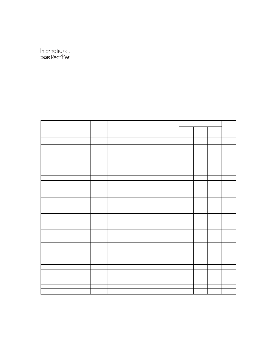
Input voltage range - -0.5Vdc to +80Vdc Input voltage range - 18Vdc to +60Vdc
Output power - Internally limited Input voltage range
1
- 18Vdc to +50Vdc
Lead temperature - +300°C for 10 seconds Output power - 0 to Max. Rated
Operating temperature - -55°C to +135°C Operating temperature
2
- -55°C to +125°C
Storage temperature - -55°C to +135°C Operating temperature
1
- -55°C to +70°C
1
Meets derating per MIL-STD-975
2
For operation at +125°C see table note 14
Absolute Maximum Ratings
Recommended Operating Conditions
Electrical Performance Characteristics
For Notes to Specifications, refer to page 4
Limits
Parameter
Group A
Subgroup
Conditions
-55
°
C
T
C
+85
°
C
V
IN
= 28V DC ± 5%, C
L
= 0
unless otherwise specified
Min
Nom
Max
Unit
Input Voltage
1,2,3
Note 2
18
28
50
V
Output Voltage ( Vout )
(main)
2812T (aux.)
2815T (aux.)
(main)
2812T (aux.)
2815T (aux.)
1
2,3
I
OUT
= 100% rated load, Note 5
I
OUT
= 100% rated load, Note 5
4.98
±11.50
±14.60
4.93
±11.30
±14.40
5.00
±11.80
±14.90
5.02
±12.10
±15.20
5.07
±12.30
±15.40
V
V
V
V
V
V
Output power ( P
OUT
)
1,2,3
V
IN
= 18, 28, 50 Volts, Note 2
0
40
W
Output current ( I
OUT
)
(main)
2812T (aux.)
2815T (aux.)
1,2,3
V
IN
= 18, 28, 50 Volts, Notes 2,3,4,5
400
83
67
4000
±833
±667
mA
mA
mA
Line regulation ( VR
LINE
)
(main)
2812T (aux.)
2815T (aux.)
1,2,3
V
IN
= 18, 28, 50 Volts
I
OUT
= 10%, 50%, 100% rated
Note 5
-10
-120
-150
10
120
150
mV
mV
mV
Load regulation ( VR
LOAD
)
(main)
2812T (aux.)
2815T (aux.)
1,2,3
I
OUT
= 10%, 50%, 100% rated
V
IN
= 18, 28, 50 Volts
Notes 5,13
-50
-400
-500
50
400
500
mV
mV
mV
Cross regulation ( VR
CROSS
)
2812T (aux.)
2815T (aux.)
1,2,3
V
IN
= 18, 28, 50 Volts
I
OUT
= 1A to 4A (main), ±416mA on (aux.)
I
OUT
= 1A to 4A (main), ±333mA on (aux.)
-3.5
-3.0
3.5
3.0
%
%
Total regulation ( VR )
(main)
2812T (aux.)
2815T (aux.)
1,2,3
All conditions of Line, Load,
and Cross Regulation, and
Temperature
4.90
±11.00
±13.50
5.10
±13.00
±16.50
V
V
V
Input current ( I
IN
)
1,2,3
I
OUT
= 0, Pin 3 open
80
mA
Pin 3 shorted to pin 2
5
Output ripple ( V
RIP
)
(main)
2812T (aux.)
2815T (aux.)
1,2,3
V
IN
= 18, 28, 50 Volts
I
OUT
= 100% rated load, Notes 5, 6
25
30
30
50
60
75
mV p-p
mV p-p
mV p-p
Switching frequency ( F )
1,2,3
Sync. Input (Pin 4) open
450
500
550
KHz
Efficiency (E
ff
)
1,2,3
I
OUT
= 100% rated load; Note 5
75
79
%
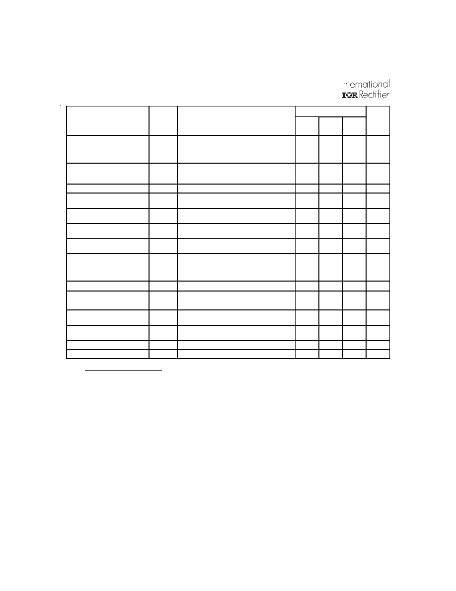
4
www.irf.com
H-SERIES
Electrical Performance Characteristics
( continued )
Limits
Parameter
Group A
Subgroup
Conditions
-55
°
C
T
C
+125
°
C
V
IN
= 28V DC ± 5%, C
L
= 0
unless otherwise specified
Min
Nom
Max
Unit
Inhibit Input
open circuit voltage
drive current ( sink )
voltage range
1,2,3
Note 1
3.0
-0.5
5.0
100
50
V
µ
A
V
Current Limit Point
Expressed as a percentage
of full rated output power
1,2,3 V
out
= 90% of Nominal, Note 5
135
%
Power dissipation, load fault (P
D
)
1,2,3
Short Circuit, Overload, Note 8
18
W
Output response to
step load changes (V
TLD
)
4,5,6
Half Load to/from Full Load, Notes 5,9
-300
300
mV pk
Recovery time,
step load changes (T
TLD
)
4,5,6
Half Load to/from Full Load, Note 5,9,10
200
µ
S
Output response to
step line changes (V
TLN
)
4,5,6
18V to/from 50V
I
OUT
= 100% rated load, Notes 1,5,11
-300
300
mV pk
Recovery time,
step line changes (T
TLN
)
4,5,6
18V to/from 50V
I
OUT
= 100% rated load, Notes 1,5,10,11
200
µ
S
Turn-on Response
Overshoot (V
OS
)
(main)
( aux. )
4,5,6
No Load, Full Load; notes 5 &12
500
750
mV
mV
Turn-on Delay (T
DLY
) 4,5,6
1
5
mS
Capacitive Load (CL)
(main)
(Each aux. output)
1
I
OUT
= 100% rated load, No effect on DC
performance, Notes 1, 5, 7
1000
200
µF
µF
Line Rejection
1
I
OUT
= 100% rated load
DC to 50KHz, Notes 1, 5
40 60 dB
Isolation
1
Input to Output or Any Pin to Case
except pin 10, test @ 500VDC
100 M
Device Weight
125
grams
MTBF
MIL-HDBK-217F2, SF, 35
°
C
1.5 x 10
6
Hours
Table I. Electrical Performance Characteristics - notes
1.
Parameter is tested as part of design characterization or after design changes. Thereafter, parameter shall be guaranteed to the limits specified.
2.
Parameter verified during line and load regulation tests.
3.
Although operation with no load is permissible, light loading on the main (+5 volt) output may cause the output voltage of the auxiliary outputs
4.
(±12 volt or ±15 volt) to drop out of regulation. It is therefore recommended that at least 200 mA or 20 percent of the total output power, whichever is
greater, be taken from the main (+5 volt) output.
5.
Although operation with no load is permissible, heavy loading on the main (+5 volt) output may cause the output voltage of the auxiliary outputs
6.
(±12 volt or ±15 volt) to rise out of regulation. It is therefore recommended that at least 50 mA or 20 percent of the total output power, whichever is
greater, be taken from the auxiliary (±12 volt or ±15 volt) outputs.
7.
Unless otherwise specified, "Rated" load is 20W on the main (+5 volt) output and 10 watts each on the auxiliary (±12 volt or ±15 volt) outputs. Load
currents of up to 5A and ±1A on the main and auxiliary outputs respectively are acceptable as long as the total output power does not to exceed 40 watts.
8.
Guaranteed for a D.C. to 20MHz bandwidth. Tested using a 20KHz to 10MHz bandwidth.
9.
Capacitive load may be any value from 0 to the maximum limit without compromising dc performance.
10.
A capacitive load in excess of the maximum limit may interfere with the proper operation of the converter's overload protection, causing erratic behavior
during turn-on.
11.
Overload power dissipation is defined as the device power dissipation with the load set such that V
OUT
= 90% of nominal.
12.
Load step transition time
10
µ
Sec.
13.
Recovery time is measured from the initiation of the transient to where V
OUT
has returned to within ±1% of
14.
its steady state value.
15.
Line step transition time
100
µ
Sec.
16.
Turn-on delay time from either a step application of input power or a logic low to a logic high transition
17.
on the inhibit pin (pin 3) to the point where V
OUT
= 90% of nominal.
18.
Load is varied for output under test while the remaining outputs are loaded at 50% of rated. Regulation relative to output voltage at 50% rated load.
19.
For operation at temperatures between +85
°
C and +125
°
C, derate the maximum input voltage linearly from 60V to 40V and the maximum output power
linearly from 100% to 75%.
www.irf.com
5
H-SERIES
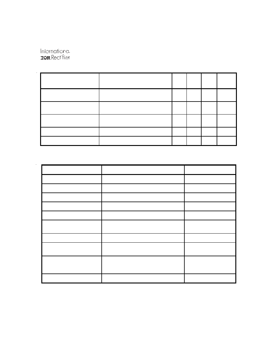
Radiation Performance Characteristics
Device Screening
Test
Conditions
Min
Typ
Highest
Level
Tested
Unit
Total Ionizing Dose ( Gamma )
MIL-STD-883, Method 1019
Operating bias applied during exposure,
Full Rated Load, V
IN
= 28V
25 40 60 Krads
(Si)
Single Event Effects
SEU, SEL, SEGR, SEB
Heavy ions (LET)
Operating bias applied during exposure,
Full Rated Load, V
IN
= 28V
37 82 82
MeV
·
cm
2
/mg
Dose Rate ( Gamma Dot )
Temporary Saturation
Survival
MIL-STD-883, Method 1023
Operating bias applied during exposure,
Full Rated Load, V
IN
= 28V
1E8
1E10
1.5E9
Rads
(Si)/sec
Neutron Fluence
MIL-STD-883, Method 1017
3E12
8E12
Neutrons
/cm
2
Proton Fluence
E > 10MeV
TBD
N/A
protons
/cm
2
Test Inspection
Method
Condition
Element Evaluation
MIL-PRF-38534 class H equivalent with SEM
Nondestructive Bond Pull
MIL-STD-883, Method 2023
Internal Visual
MIL-STD-883, Method 2017
Temperature Cycling
MIL-STD-883, Method 1010
C
Constant Acceleration
MIL-STD-883, Method 2001 (2k-g)
A, Y1 axis only
Electrical
In accordance with
device specification
Burn-in
MIL-STD-883, Method 1015
160 Hours
Final Electrical ( Group A )
In accordance with
device specification
Seal
Fine Leak
Gross Leak
MIL-STD-883, Method 1014
A1
C
External Visual
MIL-STD-883, Method 2009