Product Summary
Part Number
BV
DSS
R
DS(on)
I
D
JANTX2N6764
JANTXV2N6764
Features:
s
Avalanche Energy Rating
s
Dynamic dv/dt Rating
s
Simple Drive Requirements
s
Ease of Paralleling
s
Hermetically Sealed
N-CHANNEL
100 Volt, 0.055
HEXFET
HEXFET technology is the key to International Rectifier's
advanced line of power MOSFET transistors. The effi-
cient geometry achieves very low on-state resistance
combined with high transconductance.
HEXFET transistors also feature all of the well-establish
advantages of MOSFETs, such as voltage control, very
fast switching, ease of paralleling and electrical param-
eter temperature stability. They are well-suited for appli-
cations such as switching power supplies, motor
controls, inverters, choppers, audio amplifiers, and high
energy pulse circuits, and virtually any application where
high reliability is required.
JANTX2N6764
JANTXV2N6764
[REF:MIL-PRF-19500/543]
[GENERIC:IRF150]
HEXFET
®
POWER MOSFET
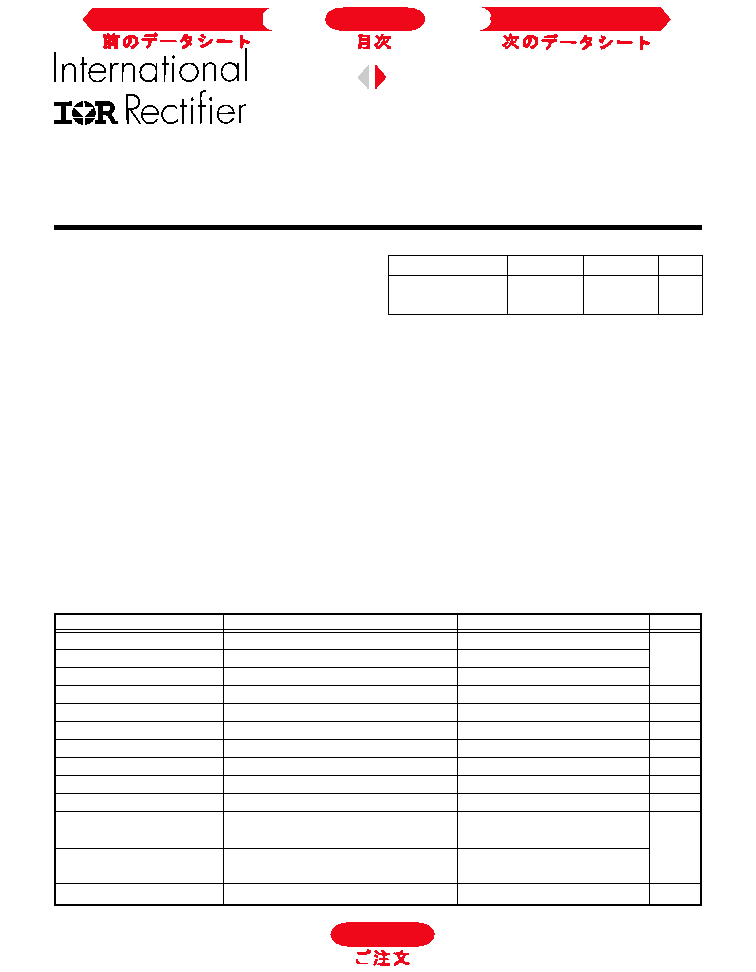
Absolute Maximum Ratings
Parameter
JANTX2N6764, JANTXV2N6764 Units
ID @ VGS = 10V, TC = 25°C
Continuous Drain Current
38
ID @ VGS = 10V, TC = 100°C Continuous Drain Current
24
IDM
Pulsed Drain Current
152
PD @ TC = 25°C
Max. Power Dissipation
150
W
Linear Derating Factor
1.2
W/K
VGS
Gate-to-Source Voltage
±20
V
EAS
Single Pulse Avalanche Energy
150
mJ
IAR
Avalanche Current
38
A
EAR
Repetitive Avalanche Energy
15
mJ
dv/dt
Peak Diode Recovery dv/dt
5.5
V/ns
TJ
Operating Junction
-55 to 150
TSTG
Storage Temperature Range
Lead Temperature
300 (0.063 in. (1.6mm) from
case for 10 seconds)
Weight
11.5 (typical)
g
o
C
A
38A
0.055
100V
Provisional Data Sheet No. PD-9.337E
Next Data Sheet
Index
Previous Datasheet
To Order

Thermal Resistance
Parameter
Min. Typ. Max. Units
Test Conditions
RthJC
Junction-to-Case
--
--
0.83
RthJA
Junction-to-Ambient
--
--
48
K/W
Typical socket mount
Source-Drain Diode Ratings and Characteristics
Parameter
Min. Typ. Max. Units
Test Conditions
IS
Continuous Source Current (Body Diode)
--
--
38
Modified MOSFET symbol showing the
ISM
Pulse Source Current (Body Diode)
--
--
152
integral reverse p-n junction rectifier.
VSD
Diode Forward Voltage
--
--
1.8
V
T
j
= 25°C, IS = 38A, VGS = 0V
trr
Reverse Recovery Time
--
--
500
ns
Tj = 25°C, IF = 38A, di/dt
100A/
µ
s
QRR
Reverse Recovery Charge
--
--
2.9
µ
C
VDD
50V
ton
Forward Turn-On Time
Intrinsic turn-on time is negligible. Turn-on speed is substantially controlled by LS + LD.
Electrical Characteristics
@ Tj = 25°C (Unless Otherwise Specified)
Parameter
Min.
Typ. Max. Units
Test Conditions
BVDSS
Drain-to-Source Breakdown Voltage
100
--
--
V
VGS = 0V, ID = 1.0 mA
BVDSS/
TJ Temperature Coefficient of Breakdown
--
0.13
--
V/°C
Reference to 25°C, ID = 1.0 mA
Voltage
RDS(on)
Static Drain-to-Source
--
--
0.055
VGS = 10V, ID = 24A
On-State Resistance
--
--
0.065
VGS = 10V, ID = 38A
VGS(th)
Gate Threshold Voltage
2.0
--
4.0
V
VDS = VGS, ID = 250
µ
A
gfs
Forward Transconductance
9
--
--
S (
)
VDS > 15V, IDS = 24A
IDSS
Zero Gate Voltage Drain Current
--
--
25
VDS = 0.8 x Max Rating,VGS = 0V
--
--
250
VDS = 0.8 x Max Rating
VGS = 0V, TJ = 125°C
IGSS
Gate-to-Source Leakage Forward
--
--
100
VGS = 20V
IGSS
Gate-to-Source Leakage Reverse
--
--
-100
VGS = -20V
Qg
Total Gate Charge
50
--
125
VGS = 10V, ID = 38A
Qgs
Gate-to-Source Charge
8
--
22
VDS = Max. Rating x 0.5
Qgd
Gate-to-Drain ("Miller") Charge
25
--
65
see figures 6 and 13
td(on)
Turn-On Delay Time
--
--
35
VDD = 50V, ID = 38A,
tr
Rise Time
--
--
190
RG = 2.35
,
VGS = 10V
td(off)
Turn-Off Delay Time
--
--
170
tf
Fall Time
--
--
130
see figure 10
LD
Internal Drain Inductance
--
5.0
--
LS
Internal Source Inductance
--
13
--
Ciss
Input Capacitance
--
3700
--
VGS = 0V, VDS = 25V
Coss
Output Capacitance
--
1100
--
f = 1.0 MHz
Crss
Reverse Transfer Capacitance
--
200
--
see figure 5
JANTX2N6764, JANTXV2N6764 Device
µ
A
nC
pF
nH
ns
Measured from the
drain lead, 6mm (0.25
in.) from package to
center of die.
Measured from the
source lead, 6mm
(0.25 in.) from package
to source bonding pad.
Modified MOSFET
symbol showing the
internal inductances.
nA
A
Next Data Sheet
Index
Previous Datasheet
To Order
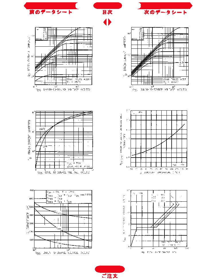
Fig. 1 -- Typical Output Characteristics
T
C
= 25°C
Fig. 2 -- Typical Output Characteristics
T
C
= 150°C
Fig. 3 -- Typical Transfer Characteristics
Fig. 4 -- Normalized On-Resistance Vs.Temperature
Fig. 5 -- Typical Capacitance Vs. Drain-to-Source
Voltage
Fig. 6 -- Typical Gate Charge Vs. Gate-to-Source
Voltage
JANTX2N6764, JANTXV2N6764 Device
To Order
Next Data Sheet
Index
Previous Datasheet
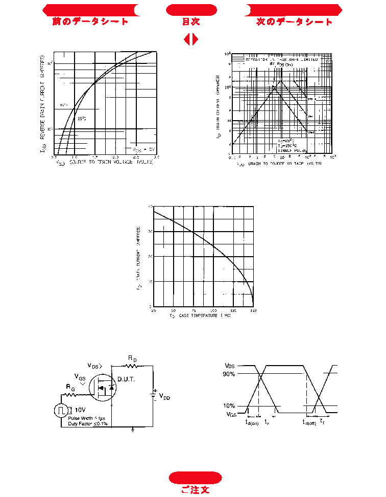
JANTX2N6764, JANTXV2N6764 Device
Fig. 10b -- Switching Time Waveforms
Fig. 10a -- Switching Time Test Circuit
Fig. 8 -- Maximum Safe Operating Area
Fig. 9 -- Maximum Drain Current Vs. Case Temperature
Fig. 7 -- Typical Source-to-Drain Diode Forward
Voltage
To Order
Next Data Sheet
Index
Previous Datasheet
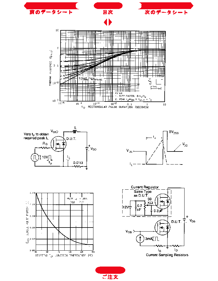
Fig. 12c -- Max. Avalanche Energy vs. Current
Fig. 13a -- Gate Charge Test Circuit
Fig. 12a -- Unclamped Inductive Test Circuit
Fig. 12b -- Unclamped Inductive Waveforms
Fig. 11 -- Maximum Effective Transient Thermal Impedance, Junction-to-Case Vs. Pulse Duration
JANTX2N6764, JANTXV2N6764 Device
To Order
Next Data Sheet
Index
Previous Datasheet