Äîêóìåíòàöèÿ è îïèñàíèÿ www.docs.chipfind.ru
1
Data Sheet PD No.60238
IRS2153D(S)PbF
SELF-OSCILLATING HALF-BRIDGE DRIVER IC
Features Product
Summary
VOFFSET 600V
Max
Duty Cycle
50%
Driver source/sink
current
180/260mA typ.
Vclamp 15.4V
typ.
Integrated 600V Half-Bridge Gate Driver
CT, RT programmable oscillator
15.4V Zener Clamp on VCC
Micropower Startup
Non-latched shutdown on CT pin (1/6th VCC)
Internal bootstrap FET
Excellent Latch Immunity on All Inputs & Outputs
+/- 50V/ns dV/dt immunity
ESD Protection on All Pins
8-lead SOIC or PDIP package
1.1 usec (typ.) internal deadtime
Deadtime
1.1us typ.
Description
The IRS2153D is based on the popular IR2153 self-
oscillating half-bridge gate driver IC using a more
advanced silicon platform, and incorporates a high
voltage half-bridge gate driver with a front end oscillator
similar to the industry standard CMOS 555 timer. HVIC
and latch immune CMOS technologies enable rugged
monolithic construction. The output driver features a high
pulse current buffer stage designed for minimum driver
cross-conduction. Noise immunity is achieved with low
di/dt peak of the gate drivers.
Package
PDIP8 SO8
IRS2153DPBF IRS2153DSPBF
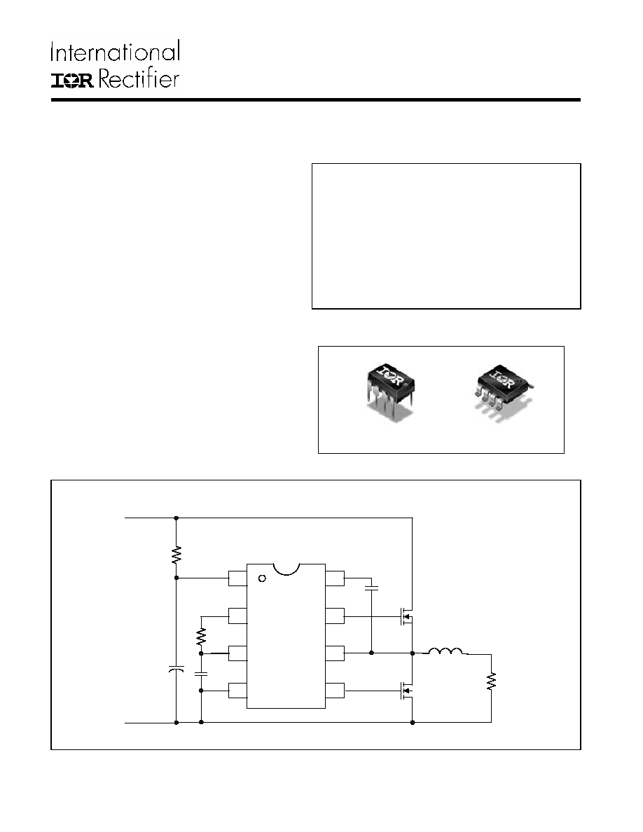
Typical Connection Diagram
RT
CT
COM
VCC
1
2
3
4
7
6
5
8
IRS2153D
LO
VS
HO
VB
CBOOT
MHS
MLS
L
RL
RVCC
RT
CT
CVCC
+ AC Rectified Line
- AC Rectified Line
2
IRS2153D(S)PbF
Absolute Maximum Ratings
Absolute Maximum Ratings indicate sustained limits beyond which damage to the device may occur. All
voltage parameters are absolute voltages referenced to COM, all currents are defined positive into any lead.
The Thermal Resistance and Power Dissipation ratings are measured under board mounted and still air
conditions.
Parameter
Symbol Definition
Min.
Max.
Units
V
B
High Side Floating Supply Voltage
-0.3
625
V
V
S
High Side Floating Supply Offset Voltage
V
B
- 25
V
B
+ 0.3
V
V
HO
High-Side Floating Output Voltage
V
S
0.3
V
B
+ 0.3
V
V
LO
Low-Side Output Voltage
-0.3
V
CC
+ 0.3
V
I
RT
R
T
Pin Current
-5
5
mA
V
RT
R
T
Pin Voltage
-0.3
V
CC
+ 0.3
V
V
CT
C
T
Pin Voltage
-0.3
V
CC
+ 0.3
V
I
CC
Supply Current (Note 1)
---
20
mA
IOMAX
Maximum allowable current at LO and HO due to external
power transistor Miller effect.
-500 500
dV
S
/dt
Allowable Offset Voltage Slew Rate
-50
50
V/ns
P
D
Maximum Power Dissipation @ T
A
+25ºC, 8-Pin DIP
--- 1.0
W
P
D
Maximum Power Dissipation @ T
A
+25ºC, 8-Pin SOIC
--- 0.625
W
R
JA
Thermal Resistance, Junction to Ambient, 8-Pin DIP
---
85
ºC/W
R
JA
Thermal Resistance, Junction to Ambient, 8-Pin SOIC
---
128
ºC/W
T
J
Junction
Temperature
-55
150
T
S
Storage
Temperature
-55
150 ºC
T
L
Lead Temperature (Soldering, 10 seconds)
---
300
Note 1: This IC contains a zener clamp structure between the chip V
CC
and COM which has a nominal
breakdown voltage of 15.4V. Please note that this supply pin should not be driven by a DC, low
impedance power source greater than the V
CLAMP
specified in the Electrical Characteristics section.
3
IRS2153D(S)PbF
Recommended Operating Conditions
For proper operation the device should be used within the recommended conditions.
Parameter
Symbol Definition
Min.
Max.
Units
V
BS
High Side Floating Supply Voltage
V
CC
- 0.7
V
CLAMP
V
V
S
Steady State High Side Floating Supply Offset Voltage
-3.0 (Note 2)
600
V
V
CC
Supply
Voltage
V
CCUV+
+0.1V V
CC CLAMP
V
I
CC
Supply Current
(Note 3)
5
mA
T
J
Junction
Temperature
-40
125 ºC
Note 2: Care should be taken to avoid output switching conditions where the V
S
node flies inductively below
ground by more than 5V.
Note 3: Enough current should be supplied to the V
CC
pin of the IC to keep the internal 15.6V zener diode
clamping the voltage at this pin.
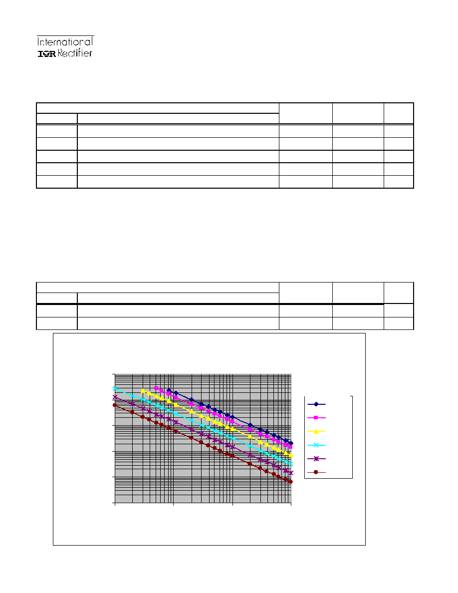
Recommended Component Values
Parameter
Symbol Component
Min.
Max.
Units
R
T
Timing Resistor Value
1
---
k
C
T
C
T
Pin Capacitor Value
330
---
pF
IRS2153D Frequency vs. RT
10
100
1000
10000
100000
1000000
1000
10000
100000
1000000
RT (Ohm)
Frequency (Hz)
330pf
470pF
1nF
2.2nF
4.7nF
10nF
CT Values
4
IRS2153D(S)PbF
Electrical Characteristics
VBIAS (V
CC
, V
BS)
= 14V, C
T
= 1 nF, VS=0V and T
A
= 25°C unless otherwise specified. The output voltage and current (V
O
and I
O)
parameters are referenced to COM and are applicable to the respective output leads: HO or LO.
Symbol Definition Min
Typ
Max
Units
Test Conditions
Low Voltage Supply Characteristics
V
CCUV+
Rising
V
CC
Undervoltage Lockout Threshold
10.2
10.8
11.5
V
CCUV-
Falling
V
CC
Undervoltage Lockout Threshold
8.3
8.8
9.4
V
V
CCUVHYS
V
CC
Undervoltage Lockout Hysteresis
1.6
2.0
2.4
I
QCCUV
Micropower Startup V
CC
Supply Current
---
130
170
µA
V
CC
V
CCUV-
I
QCC
Quiescent VCC Supply Current
---
800
1000
µA
I
CC
VCC Supply Current
---
1.8
---
mA
R
T
= 36.9k
V
CC
CLAMP
V
CC
Zener Clamp Voltage
14.4
15.4
16.8
V
I
CC
= 5mA
Floating Supply Characteristics
I
QBS
Quiescent
V
BS
Supply Current
---
60
80
µA
V
BSUV+
V
BS
Supply Undervoltage Positive Going
Threshold
8.0 9.0 9.5 V
V
BSUV-
V
BS
Supply Undervoltage negative Going
Threshold
7.0 8.0 9.0
I
LK
Offset Supply Leakage Current
---
---
50
µA
V
B
= V
S
= 600V
Oscillator I/O Characteristics
f
OSC
Oscillator
Frequency
18.4
19.0
19.6 kHz
R
T
= 36.5k
88
93
100
R
T
= 7.15k
d R
T
Pin Duty Cycle
---
50
---
%
f
o
< 100kHz
I
CT
C
T
Pin Current
---
0.02
1.0
µA
I
CTUV
UV-Mode
C
T
Pin Pulldown Current
0.20
0.30
0.6
mA
V
CC
= 7V
V
CT+
Upper
C
T
Ramp Voltage Threshold
---
9.32
---
V
CT-
Lower
C
T
Ramp Voltage Threshold
---
4.66
---
V
V
CTSD
C
T
Voltage Shutdown Threshold
2.2
2.3
2.4
V
RT+
High-Level
R
T
Output Voltage, V
CC
- V
RT
---
10
50
mV
I
RT
= -100
µA
---
100
300
mV
I
RT
= -1mA
V
RT-
Low-Level
R
T
Output Voltage
---
10
50
mV
I
RT
= 100
µA
---
100
300
mV
I
RT
= 1mA
V
RTUV
UV-Mode
R
T
Output Voltage
---
0
100
mV
V
CC
V
CCUV-
V
RTSD
SD-Mode
R
T
Output Voltage, V
CC
- V
RT
---
10
50
mV
I
RT
= -100
µA,
V
CT
= 0V
---
100
300
mV
I
RT
= -1mA,
V
CT
= 0V
5
IRS2153D(S)PbF
Electrical Characteristics
VBIAS (V
CC
, V
BS)
= 14V, C
T
= 1 nF, VS=0V and T
A
= 25°C unless otherwise specified. The output voltage and current (V
O
and I
O)
parameters are referenced to COM and are applicable to the respective output leads: HO or LO.
Symbol Definition Min
Typ
Max
Units
Test Conditions
Gate Driver Output Characteristics
V
OH
High-Level Output Voltage
---
VCC
---
I
O
= 0A
V
OL
Low-Level Output Voltage
---
COM
---
I
O
= 0A
V
OL_UV
UV-Mode Output Voltage
---
COM
---
I
O
= 0A,
V
CC
V
CCUV-
t
r
Output Rise Time
---
120
220
t
f
Output Fall Time
---
50
80
nsec
t
sd
Shutdown Propagation Delay
---
350
---
t
d
Output Deadtime (HO or LO)
0.65
1.1
1.75
µsec
IO+
Output source current
---
180
---
IO-
Output sink current
---
260
---
mA
Bootstrap FET Characteristics
VB_ON
VB when the bootstrap FET is on
---
13.7
---
V
IB_CAP
VB source current when FET is on
40
55
---
CBS=0.1uF
IB_10V
VB source current when FET is on
10
12
---
mA
VB=10V