Äîêóìåíòàöèÿ è îïèñàíèÿ www.docs.chipfind.ru
page 1
IRPT205
Revised 5/97
PD 6.073C
TM
Integrated Power Stage for 3 hp Motor Drives
IRPT2051
PRELIMINARY
· 3 hp (2.2kW) motor drive
Industrial rating at 150% overload for 1 minute
· 380 - 480V AC, 50/60Hz
· Available as complete system or sub-system assemblies
Power Module
· 3-phase rectifier bridge
· 3-phase, short circuit rated, ultrafast IGBT inverter
· Brake IGBT and diode
· Low inductance (current sense) shunts in positive and
negative DC rail
· NTC temperature sensor
· Pin-to-base plate isolation 2500V rms
· Easy-to-mount two-screw package
· Case temp. range -25° deg C to 125 deg C operational
Driver-
Plus Board
· DC bus capacitor filter with NTC inrush current limiter
· IR2233 monolithic 3-phase HVIC driver
· Driver stage for brake transistor
· On-board +15V and +5V power supply
· MOV surge suppression at input
· DC bus voltage and current feedback
· Protection for short-circuit, earth/ground fault,
overtemperature and overvoltage
· Terminal blocks for 3-phase input/output and brake
connections
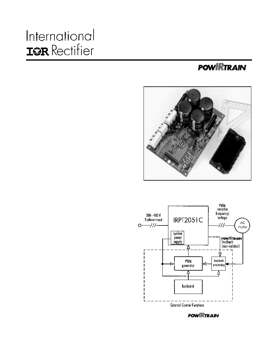
Figure 1. The IRPT2051C
within a motor
control system
page 2
IRPT2051
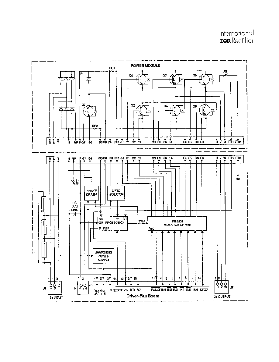
System Description
The IRPT2051C
provides the complete
power conversion function for a 3hp (2.2kW) variable-frequency,
variable-voltage, AC motor controller. The
combines a power assembly IRPT2051A with a Driver-Plus
Board IRPT2051D. Figure 1 shows the block diagram of the
within an AC motor control system.
The power module contains a 3-phase input bridge rectifier, 3-
phase IGBT and diode, 3-phase IGBT inverter, current sense
shunts, and a thermistor. It is designed for easy mounting to a
heat sink.
The Driver-Plus Board contains DC link capacitors, capacitor
soft charge function using NTC thermistor, surge suppression
MOVs, IGBT gate drivers, DC bus voltage and current feedback
signals, protection circuitry and local power supply. It is de-
signed to mate with a controller board through a single row
header. Terminal blocks are also provided on the Driver-Plus
Board for all end-user line input, motor output, and brake resis-
tor.
Output power is Pulse-Width Modulated (PWM), 3-phase,
variable-frequency, variable voltage controlled by an externally-
generated user-provided PWM controller for inverter IGBT
switching. The power supply offers the user non-isolated 5V and
15V to power the microcontroller.
The IRPT2051C offers several benefits to the drive manufac-
turer as listed below:
· It eliminates component selection, design layout, intercon-
nection, gate drive, local power supply, thermal sensing,
current sensing, and protection.
· Gate drive and protection circuits are designed to closely
match the operating characteristics of the power semicon-
ductors. This allows power losses to be minimized and
power rating to be maximized to a greater extent than is
possible by designing with individual components.
· It reduces the effort of calculating and evaluating power
semiconductor losses and junction temperature.
· It reduces the manufacturer's part inventory and simplifies
assembly.
[
specifications and ratings are given for
system input and output voltage and current, power losses
and heat sink requirements over a range of operating con-
ditions.
system ratings are verified by IR
in final testing.]
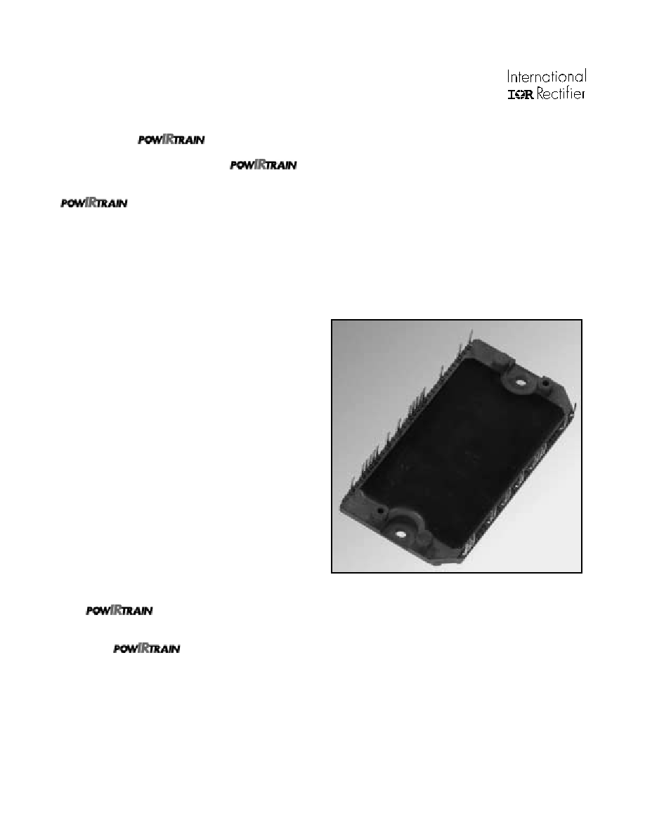
The IRPT2051A Power Module
The IRPT2051A power module, shown in figure 2, is a chip
and wire epoxy-encapsulated module. It houses input rectifiers,
brake IGBT and freewheeling diode, output inverter, current
sense shunts and NTC thermistor. The 3-phase input bridge
rectifiers are rated at 1600V. The brake circuit uses 1200V
IGBT and free-wheeling diode. The inverter section employs
1200V, short circuit rates, ultrafast IGBTs and ultrafast free-
wheeling diodes. Current sensing is achieved through 25 m
low-inductance shunts provided in the positive and negative
DC bus rail. The NTC thermistor provides temperature sensing
capability. The lead spacing on the power modulemeets UL840
pollution level 3 requirements.
Figure 2. IRPT2051A Power Module
The power circuit and layout within the module are carefully
designed to minimize inductance in the power path, to reduce
noise during inverter operation and to improve the inverter effi-
ciency. The Driver-Plus Board required to run the inverter can
be soldered to the power module pins, thus minimizing assembly
and alignment. The power module is designed to be mounted to
a heat sink with two screw mount positions, in order to insure
good thermal contact between the module substrate and the heat
sink.
page 3
IRPT2051
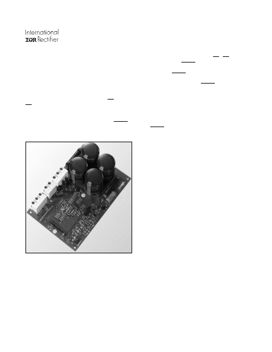
The IRPT2051D Driver-
Plus Board
The Driver-Plus Board, shown in figure 3, is the interface be-
tween the controller and the power stage. It contains the IGBT
gate drivers, protection circuitry, feedback, brake drive and local
power supply. The driver also interfaces to the AC input line. It
houses the DC link capacitors, NTC in-rush limiting thermistor,
and surge suppression MOVs.
The inverter gate drive circuits, implemented with an
IR2233 monolithic 3-phase HVIC driver, deliverrs gate drive to
the IGBTs corresponding to PWM control signals IN1 through
IN6. it introduces a 0.2 µsec dead time between upper and lower
gate signals for each phase. Any additional dead time necessary
tmust be included in the PWM signals. After a fault condition
all inverter gate drivers are disabled and latched. The FAULT
pin is also pulled low through an open drain which illuminates a
red LED. Gate drives must be enabled with an active low pulse
applied to the RESET pin while PWM inputs In1,...IN6 are held
high (off condition). The FAULT condition can also be set by
the controller through an active high signal on the STOP pin.
After power-up, the RESET pin must be pulled low before any
input signals are activated.
The protection circuitry will set a FAULT for short-circuit,
earth-fault, over-temperature, or over-voltage conditions as
specified. Current signals are sensed through shunts in positive
and negative DC bus rails. Earth faults are sensed using the
high-side shunt and the signal is fed through an opto-isolator to
the protection circuitry. Over-voltage is sensed through a resis-
tor divider from the positive DC bus. Over-temperature
protection is obtained using a thermistor inside the power mod-
ule. A FAULT condition occurs inf the temperature of the
power module's IMS substrate exceeds the trip level. The sys-
tem is designed for 150% overload for one minute while
operating with the specified heat sinks. The controller should
shut off the PWM signals if the overload persists for more than
one minute.
The feedback signals used by the protection circuitry are also
available to the controller. The current feedback signal from the
low-side shunt is available on the IFB pin at 0.025 V/A. If filter-
ing of this signal is required, it should be done by adding a
high-impedance buffer stage between signal and filter. The DC
bus reference is provided on VFB. This reference has been
scaled down by a factor of 100 and should also be protected with
a high-impedance buffer stage.
The brake function is implemented by connecting a power
resistor between the terminals on the Brake terminal block. The
value and power of theresistor determines maximum braking ca-
pability along with the rating of the brake IGBT. The input
signal on IN7 is active low and CMOS or LSTTL compatible.
The switching power supply employs an IR2152 self-oscil-
lating driver chip in a buck regulator topology to deliver a
nominal 15V and 5V DC with respect to the negative bus (N).
The power supply feeds the gate drive and protection circuits.
The 15V (V
CC
) and 5V (V
DD
) outputs are available on the con-
trol interface for powering the user's control logic.
Figure 3. IRPT2051D Driver-
Plus
Board
page 4
IRPT2051
Figure 4. IRPT2051C Basic Architecture

page 5
IRPT2051
PARAMETERS VALUES CONDITIONS
Input Power
Voltage 380V, -15%, 480V +10%
Frequency 50 - 60Hz
Input current 8.26A rms @ nominal output T
A
= 40°C, R
thSA
= 0.59°C/W
125 A peak Initial bus capacitor charging
Output Power
Voltage 0 - 480V rms defined by external PWM control
Nominal motor hp (kW) 3hp (2.2 kW) nominal full load power R
thSA
= 0.59°C/W,
150% overload for 1 minute V
in
=460V AC, f
PWM
= 4kHz,
Nominal motor current 5.90A rms nominal full load current f
°
=60Hz, T
A
= 40°C,
8.85A rms 150% overload for 1 minute Z
thSA
limits ÐT
c
to 10°C during overload
Control Inputs
IN1...IN6, (PWM), IN7 (Brake), 5V maximum, active low CMOS, LSTTL compatible,
RESET open collector
STOP 5V maximum, active high CMOS or LSTTL compatible
Pulse deadtime 0.2
µ
sec typical, set by IR2233
maximum set by controller
Minimum input pulse width 1.0
µ
sec
Protection
Output current trip level 45A peak, ±10% T
C
= 25°C
Earth fault current trip level 50A, ±10% T
C
= 25°C
Overtemperature trip level 100°C, ±5% Case temperature
Overvoltage trip level 850V, ±10%
Maximum DC link voltage 760V user to ensure rating not exceeded >30 sec
Short circuit shutdown time 2.5
µ
sec typical
output terminals shorted
Feedback Signals
Current feedback (IFB) 0.025V/A
BUS
typical T
C
= 25°C
DC bus voltage feedback (VFB)
0.010V/V
BUS
typical T
C
= 25°C
Fault feedback (FAULT) 5V maximum, active low CMOS or LSTTL compatible
On Board Power Supply
V
CC
15V, ±10%
V
DD
5V, ±5%
I
CC
+ I
DD
60 mA available to user
B r a k e
Current 10.5A
Module
Isolation voltage 2500V rms pin-to-baseplate isolation, 60Hz, 1 min.
Operating case temperature -25°C to 125°C 95% RH max. (non-condensing)
Mounting torque 1 N-m M4 screw type
System Environment
Ambient operating temp. range 0 to 40°C 95% RH max. (non-condensing)
Storage temp.range -25 to 60°C
Specifications