Äîêóìåíòàöèÿ è îïèñàíèÿ www.docs.chipfind.ru
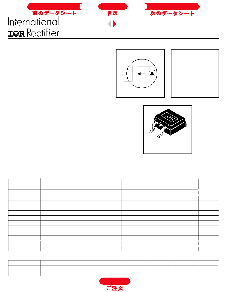
HEXFET
®
Power MOSFET
IRLZ34NS
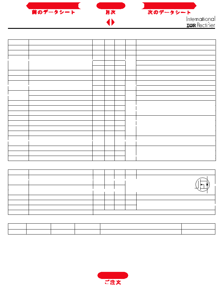
PD - 9.1308A
V
DSS
= 55V
R
DS(on)
= 0.035
I
D
= 27A
S
D
G
11/11/96
PRELIMINARY
Parameter
Min.
Typ.
Max.
Units
R
JC
Junction-to-Case
2.7
R
JA
Junction-to-Ambient (PCB Mount,steady-state)**
40
Thermal Resistance
°C/W
l
Logic-Level Gate Drive
l
Advanced Process Technology
l
Surface Mount
l
Dynamic dv/dt Rating
l
175°C Operating Temperature
l
Fast Switching
l
Fully Avalanche Rated
Parameter
Max.
Units
I
D
@ T
C
= 25°C
Continuous Drain Current, V
GS
@ 10V
27
I
D
@ T
C
= 100°C
Continuous Drain Current, V
GS
@ 10V
19
A
I
DM
Pulsed Drain Current
110
P
D
@T
C
= 25°C
Power Dissipation
56
W
Linear Derating Factor
0.37
W/°C
V
GS
Gate-to-Source Voltage
±16
V
E
AS
Single Pulse Avalanche Energy
110
mJ
I
AR
Avalanche Current
16
A
E
AR
Repetitive Avalanche Energy
5.6
mJ
dv/dt
Peak Diode Recovery dv/dt
10
V/ns
T
J
Operating Junction and
-55 to + 175
T
STG
Storage Temperature Range
°C
Soldering Temperature, for 10 seconds
300 (1.6mm from case)
Absolute Maximum Ratings
Fifth Generation HEXFETs from International Rectifier
utilize advanced processing techniques to achieve the
lowest possible on-resistance per silicon area. This benefit,
combined with the fast switching speed and ruggedized
device design that HEXFET Power MOSFETs are well
known for, provides the designer with an extremely efficient
device for use in a wide variety of applications.
The D
2
Pak is a surface mount power package capable of
accommodating die sizes up to HEX-4. It provides the
highest power capability and the lowest possible on-
resistance in any existing surface mount package. The
D
2
Pak is suitable for high current applications because of
its low internal connection resistance and can dissipate up
to 2.0W in a typical surface mount application.
Description
2
D Pak
Next Data Sheet
Index
Previous Datasheet
To Order
IRLZ34NS
Parameter
Min. Typ. Max. Units
Conditions
V
(BR)DSS
Drain-to-Source Breakdown Voltage
55
V
V
GS
= 0V, I
D
= 250µA
V
(BR)DSS
/
T
J
Breakdown Voltage Temp. Coefficient
0.065
V/°C
Reference to 25°C, I
D
= 1mA
0.035
V
GS
= 10V, I
D
= 16A
V
GS
= 5.0V, I
D
= 16A
0.060
V
GS
= 4.0V, I
D
= 14A
V
GS(th)
Gate Threshold Voltage
1.0
2.0
V
V
DS
= V
GS
, I
D
= 250µA
g
fs
Forward Transconductance
11
S
V
DS
= 25V, I
D
= 16A
25
V
DS
= 55V, V
GS
= 0V
250
V
DS
= 44V, V
GS
= 0V, T
J
= 150°C
Gate-to-Source Forward Leakage
100
V
GS
= 16V
Gate-to-Source Reverse Leakage
-100
V
GS
= -16V
Q
g
Total Gate Charge
25
I
D
= 16A
Q
gs
Gate-to-Source Charge
5.2
nC
V
DS
= 44V
Q
gd
Gate-to-Drain ("Miller") Charge
14
V
GS
= 5.0V, See Fig. 6 and 13
t
d(on)
Turn-On Delay Time
8.9
V
DD
= 28V
t
r
Rise Time
100
I
D
= 16A
t
d(off)
Turn-Off Delay Time
29
R
G
= 6.5
,
V
GS
= 5.0V
t
f
Fall Time
21
R
D
= 1.8
,
See Fig. 10
Between lead,
and center of die contact
C
iss
Input Capacitance
880
V
GS
= 0V
C
oss
Output Capacitance
220
pF
V
DS
= 25V
C
rss
Reverse Transfer Capacitance
94
= 1.0MHz, See Fig. 5
Electrical Characteristics @ T
J
= 25°C (unless otherwise specified)
I
GSS
µA
nA
ns
R
DS(on)
Static Drain-to-Source On-Resistance
0.046
I
DSS
Drain-to-Source Leakage Current
nH
L
S
Internal Source Inductance
7.5
Parameter
Min. Typ. Max. Units
Conditions
I
S
Continuous Source Current
MOSFET symbol
(Body Diode)
showing the
I
SM
Pulsed Source Current
integral reverse
(Body Diode)
p-n junction diode.
V
SD
Diode Forward Voltage
1.3
V
T
J
= 25°C, I
S
= 16A, V
GS
= 0V
t
rr
Reverse Recovery Time
76
110
ns
T
J
= 25°C, I
F
= 16A
Q
rr
Reverse RecoveryCharge
190
290
nC
di/dt = 100A/µs
t
on
Forward Turn-On Time
Intrinsic turn-on time is negligible (turn-on is dominated by L
S
+L
D
)
Source-Drain Ratings and Characteristics
A
110
27
S
D
G
Repetitive rating; pulse width limited by
max. junction temperature. ( See fig. 11 )
I
SD
16A, di/dt
270A/µs, V
DD
V
(BR)DSS
,
T
J
175°C
Notes:
V
DD
= 25V, starting T
J
= 25°C, L = 610µH
R
G
= 25
, I
AS
= 16A. (See Figure 12)
Pulse width
300µs; duty cycle
2%.
** When mounted on FR-4 board using minimum recommended footprint.
For recommended footprint and soldering techniques refer to application note #AN-994.
Uses IRLZ34N data and test conditions
Rev. #
Parameters Old spec.
New spec.
Comments
Revision Date
1
V
GS
(Max.)
±20
±16
Decrease V
GS
(
Max). Specification
5/1/96
Specification changes
Next Data Sheet
Index
Previous Datasheet
To Order
IRLZ34NS
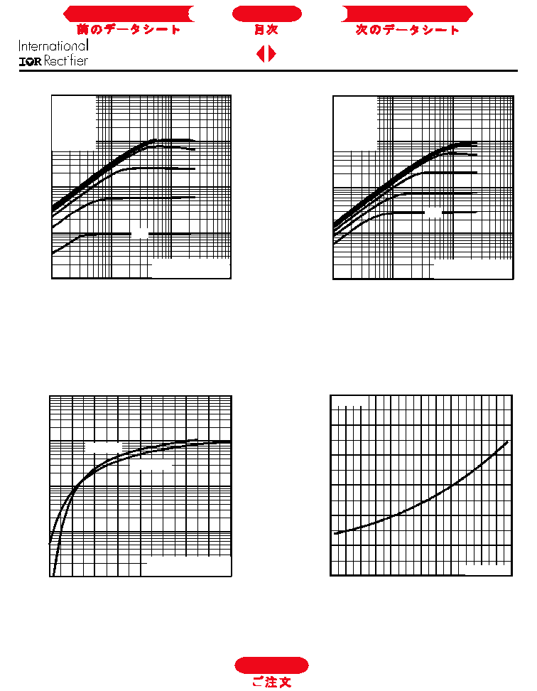
Fig 1. Typical Output Characteristics
Fig 3. Typical Transfer Characteristics
Fig 4. Normalized On-Resistance
Vs. Temperature
Fig 2. Typical Output Characteristics
0.1
1
10
100
1000
0.1
1
10
100
I
, D
r
a
i
n
-
to
-
S
o
u
r
c
e
C
u
r
r
e
n
t
(
A
)
D
V , Drain -to -S o urce Vo lta ge (V )
D S
A
2 0µ s PU L SE W ID TH
T = 1 75 °C
VGS
TOP 15V
12V
10V
8.0V
6.0V
4.0V
3.0V
BOTTOM 2.5V
2.5 V
J
0.1
1
10
100
1000
0.1
1
10
100
I
, D
r
a
i
n
-
to
-
S
o
u
r
c
e
C
u
r
r
e
n
t
(
A
)
D
V , Drain -to -S ou rce V oltag e (V)
D S
A
2 0µ s PU LSE W ID TH
T = 25 °C
J
VGS
TOP 15V
12V
10V
8.0V
6.0V
4.0V
3.0V
BOT TOM 2.5V
2.5 V
0 . 1
1
1 0
1 0 0
1 0 0 0
2
3
4
5
6
7
8
9
1 0
T = 2 5 ° C
J
G S
V , Ga te -to -S o u rce V o l ta g e (V )
D
I
, D
r
a
i
n
-
to
-
S
o
u
r
c
e
C
u
r
r
e
n
t
(
A
)
T = 1 7 5° C
J
A
V = 2 5 V
2 0 µ s P U L SE W ID TH
DS
0 . 0
0 . 5
1 . 0
1 . 5
2 . 0
2 . 5
3 . 0
- 6 0
- 4 0
- 2 0
0
2 0
4 0
6 0
8 0
1 0 0 1 2 0 1 4 0 1 6 0 1 8 0
J
T , Ju nction T em pe rature (°C )
R
,
D
r
a
i
n
-
to
-
S
o
u
r
c
e
O
n
R
e
s
i
s
t
a
n
c
e
D
S
(
on)
(
N
o
r
m
a
l
i
z
ed)
V = 10 V
G S
A
I = 2 7A
D
To Order
Next Data Sheet
Index
Previous Datasheet
IRLZ34NS
Fig 7. Typical Source-Drain Diode
Forward Voltage
Fig 5. Typical Capacitance Vs.
Drain-to-Source Voltage
Fig 8. Maximum Safe Operating Area
Fig 6. Typical Gate Charge Vs.
Gate-to-Source Voltage
0
200
400
600
800
1000
1200
1400
1
10
100
C
,
C
a
pac
i
t
anc
e (
p
F
)
D S
V , D rain-to -S ou rce Volta ge (V )
A
V = 0 V, f = 1M H z
C = C + C , C SH OR TE D
C = C
C = C + C
G S
is s gs gd ds
rss gd
oss d s gd
C
i s s
C
o s s
C
rs s
0
3
6
9
12
15
0
4
8
12
16
20
24
28
32
Q , T otal Ga te C harg e (nC )
G
V
,
G
a
t
e
-
t
o-
S
o
u
r
c
e
V
o
l
t
ag
e (
V
)
GS
A
FO R TEST CI R CU I T
SEE FIG UR E 13
I = 16A
V = 44V
V = 28V
D
DS
DS
1
1 0
1 0 0
1 0 0 0
0 . 4
0 . 6
0 . 8
1 . 0
1 . 2
1 . 4
1 . 6
1 . 8
2 . 0
T = 2 5°C
J
V = 0 V
G S
V , S o urce-to -Drain Vo lta ge (V )
I
, R
e
v
e
r
s
e
D
r
a
i
n
C
u
r
r
e
n
t
(
A
)
S D
SD
A
T = 17 5°C
J
1
10
100
1000
1
10
100
V , Dra in -to-So urce Vo ltag e (V)
D S
I
,
D
r
ai
n C
u
r
r
en
t
(
A
)
OPE R ATIO N IN TH IS A RE A LI MI TE D
BY R
D
D S(o n)
10µ s
1 00µs
1m s
10m s
A
T = 25 °C
T = 17 5°C
S ing le Pulse
C
J
To Order
Next Data Sheet
Index
Previous Datasheet
IRLZ34NS
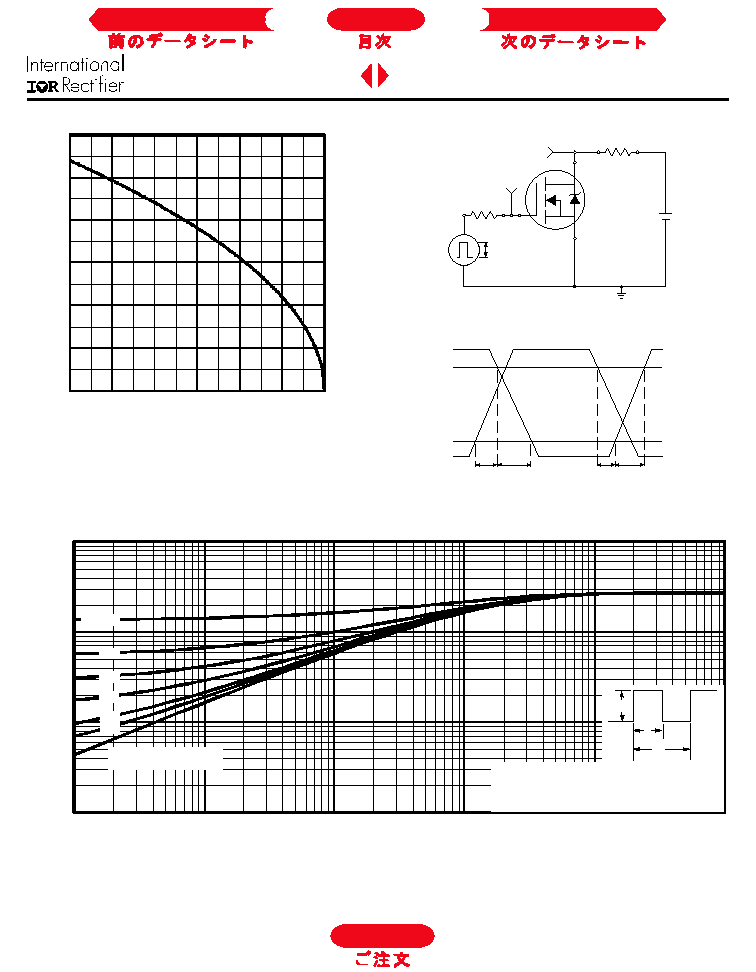
Fig 10a. Switching Time Test Circuit
V
DS
90%
10%
V
GS
t
d(on)
t
r
t
d(off)
t
f
Fig 10b. Switching Time Waveforms
Fig 11. Maximum Effective Transient Thermal Impedance, Junction-to-Case
V
DS
Pulse Width
1
µs
Duty Factor
0.1 %
R
D
V
GS
R
G
D.U.T.
5.0V
+
-
V
DD
Fig 9. Maximum Drain Current Vs.
Case Temperature
0
5
1 0
1 5
2 0
2 5
3 0
2 5
5 0
7 5
1 0 0
1 2 5
1 5 0
1 7 5
C
I
,
D
r
ai
n
C
u
r
r
ent
(
A
m
p
s
)
D
T , C ase T em pe ra ture (°C )
A
0.01
0.1
1
10
0.00001
0.0001
0.001
0.01
0.1
1
t , Rectangular Pulse Duration (sec)
1
th
J
C
D = 0.5 0
0.01
0.02
0.05
0 .1 0
0.2 0
S IN G LE P U LS E
(T H E R M A L R E S P O NS E )
A
Ther
m
a
l
R
e
sponse (
Z
)
P
t
2
1
t
D M
N o te s :
1 . D u ty fac to r D = t / t
2 . P e a k T = P x Z + T
1
2
J
D M
th J C
C
To Order
Next Data Sheet
Index
Previous Datasheet