Äîêóìåíòàöèÿ è îïèñàíèÿ www.docs.chipfind.ru
www.irf.com
1
12/7/04
HEXFET
®
Power MOSFET
V
DSS
R
DS(on)
max
Q
g
12V
8.5m
27nC
Notes
through are on page 9
PD - 95089A
Parameter
Typ.
Max.
Units
R
JC
Junction-to-Case
1.7
R
JA
Junction-to-Ambient (PCB mount)*
40
°C/W
R
JA
Junction-to-Ambient
110
Thermal Resistance
Absolute Maximum Ratings
Symbol
Parameter
Max.
Units
V
DS
Drain-Source Voltage
12
V
V
GS
Gate-to-Source Voltage
± 12 V
I
D
@ T
C
= 25°C
Continuous Drain Current, V
GS
@ 4.5V
84
I
D
@ T
C
= 100°C
Continuous Drain Current, V
GS
@ 4.5V
60
A
I
DM
Pulsed Drain Current
320
P
D
@T
C
= 25°C
Maximum Power Dissipation
88
W
P
D
@T
C
= 100°C
Maximum Power Dissipation
44
W
Linear Derating Factor 0.59 mW/°C
T
J
, T
STG
Junction and Storage Temperature Range
-55 to + 175
°C
Applications
Benefits
l
Ultra-Low Gate Impedance
l
Very Low R
DS(on)
l
Fully Characterized Avalanche Voltage
and Current
l
High Frequency 3.3V and 5V input Point-
of-Load Synchronous Buck Converters
l
Power Management for Netcom,
Computing and Portable Applications.
l
Lead-Free
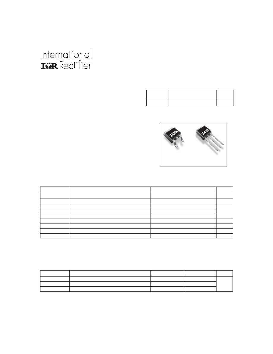
D-Pak
I-Pak
IRLR3802 IRLU3802
IRLR3802PbF
IRLU3802PbF
IRLR/U3802PbF
2
www.irf.com
Symbol
Parameter
Min. Typ. Max. Units
Conditions
I
S
Continuous Source Current
MOSFET symbol
(Body Diode)
showing the
I
SM
Pulsed Source Current
integral reverse
(Body Diode)
p-n junction diode.
0.81
1.2
V
T
J
= 25°C, I
S
= 12A, V
GS
= 0V
0.65
T
J
= 125°C, I
S
= 12A, V
GS
= 0V
t
rr
Reverse Recovery Time
52
78
ns
T
J
= 25°C, I
F
= 12A, V
R
=20V
Q
rr
Reverse Recovery Charge
54
81
nC
di/dt = 100A/µs
t
rr
Reverse Recovery Time
50
75
ns
T
J
= 125°C, I
F
= 12A, V
R
=20V
Q
rr
Reverse Recovery Charge
50
75
nC
di/dt = 100A/µs
S
D
G
Diode Characteristics
84
320
A
V
SD
Diode Forward Voltage
Parameter
Min. Typ. Max. Units
Conditions
BV
DSS
Drain-to-Source Breakdown Voltage
12
V
V
GS
= 0V, I
D
= 250µA
V
DSS
/
T
J
Breakdown Voltage Temp. Coefficient
0.009 V/°C Reference to 25°C, I
D
= 1mA
6.5
8.5
V
GS
= 4.5V, I
D
= 15A
30
V
GS
= 2.8V, I
D
= 12A
V
GS(th)
Gate Threshold Voltage
0.6
1.9
V
V
DS
= V
GS
, I
D
= 250µA
V
GS(th)
/
T
J
Gate Threshold Voltage Coefficient
-3.2 mV/°C
100
µA
V
DS
= 9.6V, V
GS
= 0V
250
V
DS
= 9.6V, V
GS
= 0V, T
J
= 125°C
Gate-to-Source Forward Leakage
200
V
GS
= 12V
Gate-to-Source Reverse Leakage
-200
nA
V
GS
= -12V
g
fs
Forward Transconductance
31
S
V
DS
= 6.0V, I
D
= 12A
Q
g
Total Gate Charge
27 41
Q
gs1
Pre-Vth Gate-Source Charge
3.6
V
DS
= 6.0V
Q
gs2
Post-Vth Gate-Source Charge
2.0
V
GS
= 5.0V
Q
gd
Gate-to-Drain Charge
10
nC
I
D
= 6.0A
Q
godr
Gate Charge Overdrive
11
See Fig.16
Q
sw
Switch Charge (Q
gs2
+
Q
gd
)
12
Q
oss
Output Charge
28
nC
V
DS
= 10V, V
GS
= 0V
t
d(on)
Turn-On Delay Time
11
V
DD
= 6.0V, V
GS
= 4.5V
t
r
Rise Time
14
ns
I
D
= 12A
t
d(off)
Turn-Off Delay Time
21
Clamped Inductive Load
t
f
Fall Time
17
C
iss
Input Capacitance
2490
V
GS
= 0V
C
oss
Output Capacitance
2150
pF
V
DS
= 6.0V
C
rss
Reverse Transfer Capacitance
530
= 1.0MHz
Static @ T
J
= 25°C (unless otherwise specified)
I
GSS
I
DSS
Drain-to-Source Leakage Current
m
R
DS(on)
Static Drain-to-Source On-Resistance
Symbol
Parameter
Typ.
Max.
Units
E
AS
Single Pulse Avalanche Energy
300
mJ
I
AR
Avalanche Current
20
A
Avalanche Characteristics
IRLR/U3802PbF
www.irf.com
3
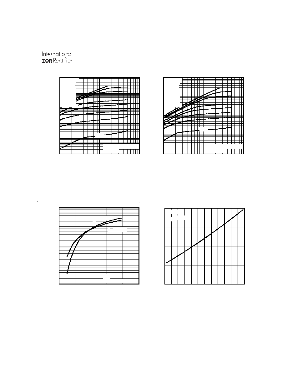
Fig 4. Normalized On-Resistance
Vs. Temperature
Fig 2. Typical Output Characteristics
Fig 1. Typical Output Characteristics
Fig 3. Typical Transfer Characteristics
0.1
1
10
VDS, Drain-to-Source Voltage (V)
0.01
0.1
1
10
100
1000
I D
,
D
r
a
i
n
-
t
o
-
S
o
u
r
c
e
C
u
r
r
e
n
t
(
A
)
1.5V
20µs PULSE WIDTH
Tj = 25°C
VGS
TOP 10V
4.5V
3.5V
2.5V
2.3V
2.0V
1.8V
BOTTOM 1.5V
0.1
1
10
VDS, Drain-to-Source Voltage (V)
0.1
1
10
100
1000
I D
,
D
r
a
i
n
-
t
o
-
S
o
u
r
c
e
C
u
r
r
e
n
t
(
A
)
1.5V
20µs PULSE WIDTH
Tj = 175°C
VGS
TOP 10V
4.5V
3.5V
2.5V
2.3V
2.0V
1.8V
BOTTOM 1.5V
1.0
2.0
3.0
4.0
5.0
6.0
VGS, Gate-to-Source Voltage (V)
0
1
10
100
1000
I D
,
D
r
a
i
n
-
t
o
-
S
o
u
r
c
e
C
u
r
r
e
n
t
(
)
TJ = 25°C
TJ = 175°C
VDS = 5.0V
20µs PULSE WIDTH
-60 -40 -20 0
20 40 60 80 100 120 140 160 180
TJ , Junction Temperature (°C)
0.5
1.0
1.5
R
D
S
(
o
n
)
,
D
r
a
i
n
-
t
o
-
S
o
u
r
c
e
O
n
R
e
s
i
s
t
a
n
c
e
(
N
o
r
m
a
l
i
z
e
d
)
ID = 84A
VGS = 4.5V
IRLR/U3802PbF
4
www.irf.com
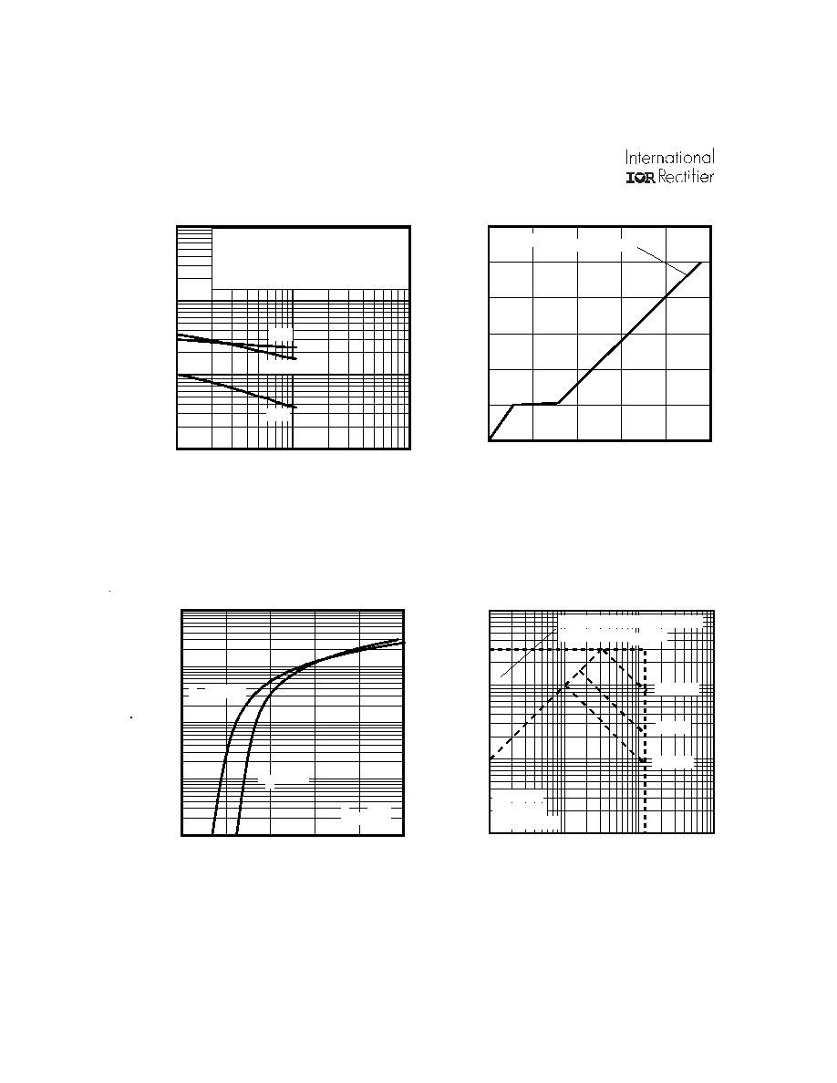
Fig 8. Maximum Safe Operating Area
Fig 6. Typical Gate Charge Vs.
Gate-to-Source Voltage
Fig 5. Typical Capacitance Vs.
Drain-to-Source Voltage
Fig 7. Typical Source-Drain Diode
Forward Voltage
1
10
100
VDS, Drain-to-Source Voltage (V)
100
1000
10000
100000
C
,
C
a
p
a
c
i
t
a
n
c
e
(
p
F
)
Coss
Crss
Ciss
VGS = 0V, f = 1 MHZ
Ciss = Cgs + Cgd, Cds SHORTED
Crss = Cgd
Coss = Cds + Cgd
0
10
20
30
40
50
QG Total Gate Charge (nC)
0
2
4
6
8
10
12
V
G
S
,
G
a
t
e
-
t
o
-
S
o
u
r
c
e
V
o
l
t
a
g
e
(
V
)
VDS= 12V
ID= 6.0A
0
1
10
100
VDS , Drain-toSource Voltage (V)
1
10
100
1000
I D
,
D
r
a
i
n
-
t
o
-
S
o
u
r
c
e
C
u
r
r
e
n
t
(
A
)
Tc = 25°C
Tj = 175°C
Single Pulse
1msec
10msec
OPERATION IN THIS AREA
LIMITED BY RDS(on)
100µsec
0.0
0.5
1.0
1.5
2.0
2.5
VSD, Source-toDrain Voltage (V)
0.1
1.0
10.0
100.0
1000.0
I S
D
,
R
e
v
e
r
s
e
D
r
a
i
n
C
u
r
r
e
n
t
(
A
)
TJ = 25°C
TJ = 175°C
VGS = 0V
IRLR/U3802PbF
www.irf.com
5
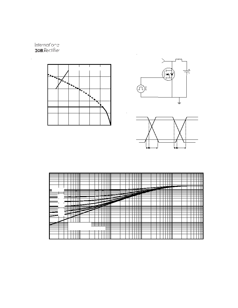
Fig 10a. Switching Time Test Circuit
Fig 10b. Switching Time Waveforms
Fig 11. Maximum Effective Transient Thermal Impedance, Junction-to-Case
Fig 9. Maximum Drain Current Vs.
Case Temperature
1E-006
1E-005
0.0001
0.001
0.01
0.1
t1 , Rectangular Pulse Duration (sec)
0.001
0.01
0.1
1
10
T
h
e
r
m
a
l
R
e
s
p
o
n
s
e
(
Z
t
h
J
C
)
0.20
0.10
D = 0.50
0.02
0.01
0.05
SINGLE PULSE
( THERMAL RESPONSE )
25
50
75
100
125
150
175
TC , Case Temperature (°C)
0
20
40
60
80
100
I D
,
D
r
a
i
n
C
u
r
r
e
n
t
(
A
)
LIMITED BY PACKAGE
V
GS
V
DS
90%
10%
t
d(on)
t
d(off)
t
f
t
r
V
GS
Pulse Width < 1µs
Duty Factor < 0.1%
V
DD
V
DS
L
D
D.U.T