IRLML6302.pmd
PD - 91259E
HEXFET
®
Power MOSFET
V
DSS
= -20V
R
DS(on)
= 0.60
Fifth Generation HEXFETs from International Rectifier
utilize advanced processing techniques to achieve
extremely low on-resistance per silicon area. This benefit,
combined with the fast switching speed and ruggedized
device design that HEXFET Power MOSFETs are well
known for, provides the designer with an extremely efficient
and reliable device for use in a wide variety of applications.
A customized leadframe has been incorporated into the
standard SOT-23 package to produce a HEXFET Power
MOSFET with the industry's smallest footprint. This
package, dubbed the Micro3, is ideal for applications
where printed circuit board space is at a premium. The low
profile (<1.1mm) of the Micro3 allows it to fit easily into
extremely thin application environments such as portable
electronics and PCMCIA cards.
IRLML6302
04/29/03
Description
l
Generation V Technology
l
Ultra Low On-Resistance
l
P-Channel MOSFET
l
SOT-23 Footprint
l
Low Profile (<1.1mm)
l
Available in Tape and Reel
l
Fast Switching
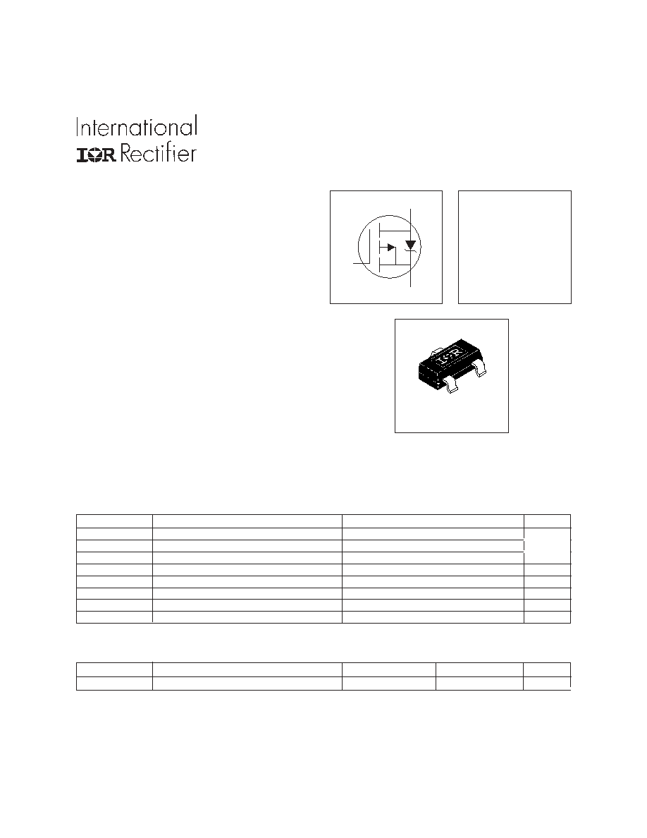
S
D
G
Micro3
Parameter
Max.
Units
I
D
@ T
A
= 25°C
Continuous Drain Current, V
GS
@ -4.5V
-0.78
I
D
@ T
A
= 70°C
Continuous Drain Current, V
GS
@ -4.5V
-0.62
A
I
DM
Pulsed Drain Current
-4.9
P
D
@T
A
= 25°C
Power Dissipation
540
mW
Linear Derating Factor
4.3
mW/°C
V
GS
Gate-to-Source Voltage
± 12
V
dv/dt
Peak Diode Recovery dv/dt
-5.0
V/ns
T
J,
T
STG
Junction and Storage Temperature Range
-55 to + 150
°C
Absolute Maximum Ratings
Parameter
Typ.
Max.
Units
R
JA
Maximum Junction-to-Ambient
230
Thermal Resistance
°C/W
IRLML6302
Parameter
Min. Typ. Max. Units
Conditions
V
(BR)DSS
Drain-to-Source Breakdown Voltage
-20
V
V
GS
= 0V, I
D
= -250µA
V
(BR)DSS
/T
J
Breakdown Voltage Temp. Coefficient
-4.9 mV/°C Reference to 25°C, I
D
= -1mA
0.60
V
GS
= -4.5V, I
D
= -0.61A
0.90
V
GS
= -2.7V, I
D
= -0.31A
V
GS(th)
Gate Threshold Voltage
-0.70
V
V
DS
= V
GS
, I
D
= -250µA
g
fs
Forward Transconductance
0.56
S
V
DS
= -10V, I
D
= -0.31A
-1.0
V
DS
= -16V, V
GS
= 0V
-25
V
DS
= -16V, V
GS
= 0V, T
J
= 125°C
Gate-to-Source Forward Leakage
-100
V
GS
= -12V
Gate-to-Source Reverse Leakage
100
V
GS
= 12V
Q
g
Total Gate Charge
2.4
3.6
I
D
= -0.61A
Q
gs
Gate-to-Source Charge
0.56 0.84
nC
V
DS
= -16V
Q
gd
Gate-to-Drain ("Miller") Charge
1.0
1.5
V
GS
= -4.5V, See Fig. 6 and 9
t
d(on)
Turn-On Delay Time
13
V
DD
= -10V
t
r
Rise Time
18
I
D
= -0.61A
t
d(off)
Turn-Off Delay Time
22
R
G
= 6.2
t
f
Fall Time
22
R
D
= 16, See Fig. 10
C
iss
Input Capacitance
97
V
GS
= 0V
C
oss
Output Capacitance
53
pF
V
DS
= -15V
C
rss
Reverse Transfer Capacitance
28
= 1.0MHz, See Fig. 5
µA
nA
ns
I
GSS
I
DSS
Drain-to-Source Leakage Current
R
DS(ON)
Static Drain-to-Source On-Resistance
Electrical Characteristics @ T
J
= 25°C (unless otherwise specified)
Parameter
Min. Typ. Max. Units
Conditions
I
S
Continuous Source Current
MOSFET symbol
(Body Diode)
showing the
I
SM
Pulsed Source Current
integral reverse
(Body Diode)
p-n junction diode.
V
SD
Diode Forward Voltage
-1.2
V
T
J
= 25°C, I
S
= -0.61A, V
GS
= 0V
t
rr
Reverse Recovery Time
35
53
ns
T
J
= 25°C, I
F
= -0.61A
Q
rr
Reverse RecoveryCharge
26
39
nC
di/dt = 100A/µs
Source-Drain Ratings and Characteristics
A
S
D
G
-4.9
-0.54
Repetitive rating; pulse width limited by
max. junction temperature. ( See fig. 11 )
I
SD
-0.61A, di/dt 76A/µs, V
DD
V
(BR)DSS
,
T
J
150°C
Notes:
Pulse width 300µs; duty cycle 2%.
Surface mounted on FR-4 board, t 5sec.
IRLML6302
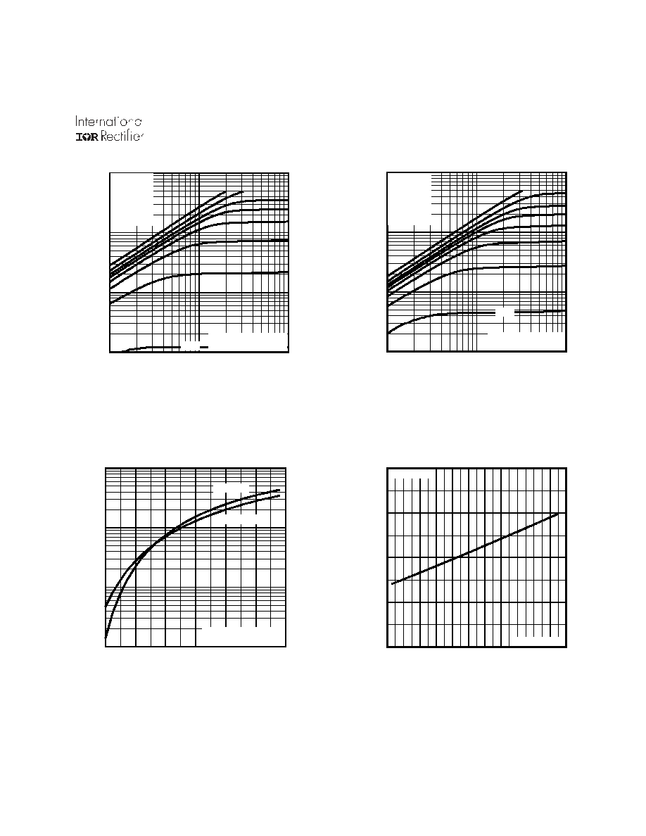
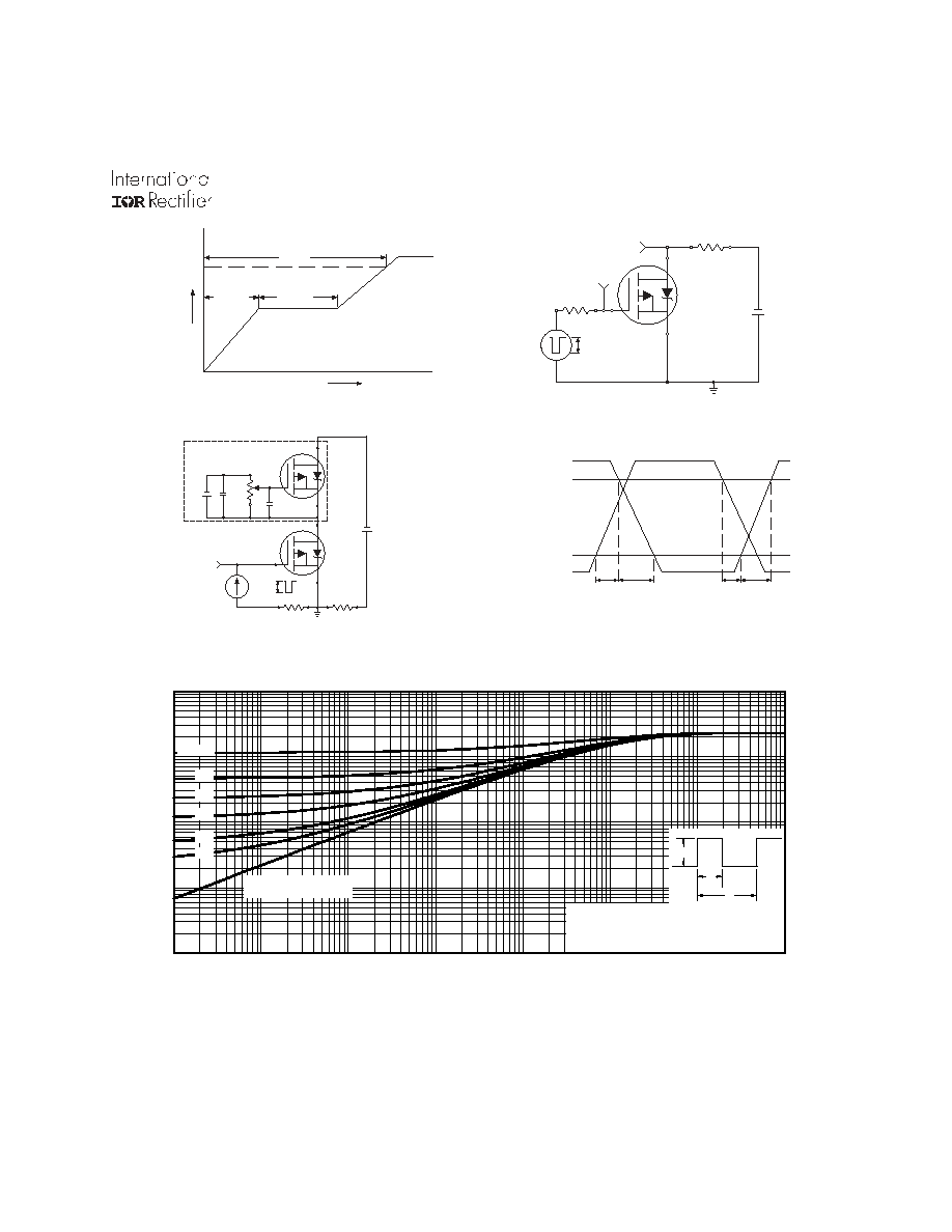
Fig 1. Typical Output Characteristics
Fig 3. Typical Transfer Characteristics
Fig 2. Typical Output Characteristics
Fig 4. Normalized On-Resistance
Vs. Temperature
0.01
0.1
1
10
0.1
1
10
D
DS
20µs PULSE WIDTH
T = 25°C
A
-I , D
r
a
i
n
-
to
-
S
o
u
rc
e
C
u
rr
e
n
t (A
)
-V , Drain-to-Source Voltage (V)
J
-1.5V
VGS
TOP - 7.5V
- 5.0V
- 4.0V
- 3.5V
- 3.0V
- 2.5V
- 2.0V
BOTTOM - 1.5V
0.01
0.1
1
10
0.1
1
10
D
DS
20µs PULSE WIDTH
T = 150°C
A
-I , D
r
a
i
n
-
to
-S
o
u
rce
C
u
rren
t
(A
)
-V , Drain-to-Source Voltage (V)
J
VGS
TOP - 7.5V
- 5.0V
- 4.0V
- 3.5V
- 3.0V
- 2.5V
- 2.0V
BOTTOM - 1.5V
-1.5V
0.01
0.1
1
10
1.5
2.0
2.5
3.0
3.5
4.0
4.5
T = 25°C
T = 150°C
J
J
GS
D
A
-I
,
Dra
i
n
-
t
o
-S
o
u
rc
e
C
u
rre
n
t
(A)
-V , Gate-to-Source Voltage (V)
V = -10V
20µs PULSE WIDTH
DS
0.0
0.5
1.0
1.5
2.0
-60 -40
-20
0
20
40
60
80
100 120 140 160
J
T , Junction Temperature (°C)
R
, D
r
a
i
n
-
to
-S
o
u
rc
e
O
n
R
e
s
i
s
t
a
n
c
e
DS
(
o
n)
(
N
or
m
a
l
i
z
ed)
A
I = -0.61A
V = -4.5V
D
GS
IRLML6302
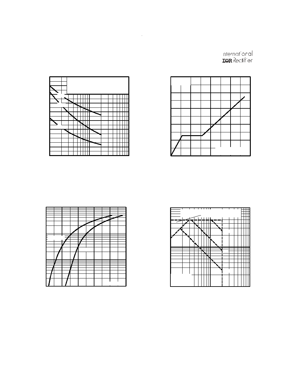
Fig 5. Typical Capacitance Vs.
Drain-to-Source Voltage
Fig 7. Typical Source-Drain Diode
Forward Voltage
Fig 8. Maximum Safe Operating Area
Fig 6. Typical Gate Charge Vs.
Gate-to-Source Voltage
0
20
40
60
80
100
120
140
160
180
1
10
100
C
,
Ca
pa
c
i
t
a
n
c
e (
p
F)
A
DS
-V , Drain-to-Source Voltage (V)
V = 0V, f = 1MHz
C = C + C , C SHORTED
C = C
C = C + C
GS
iss gs gd ds
rss gd
oss ds gd
C
iss
C
oss
C
rss
0
2
4
6
8
10
0.0
1.0
2.0
3.0
4.0
G
GS
A
-V
, G
a
te
-to
-
S
o
u
r
c
e
V
o
lta
g
e
(V
)
Q , Total Gate Charge (nC)
I = -0.61A
V = -16V
FOR TEST CIRCUIT
SEE FIGURE 9
D
DS
0.01
0.1
1
10
0.4
0.6
0.8
1.0
1.2
1.4
T = 25°C
T = 150°C
J
J
V = 0V
GS
SD
SD
A
-I , R
e
ve
rse D
r
ain
C
u
rren
t
(A
)
-V , Source-to-Drain Voltage (V)
0.1
1
10
1
10
100
OPERATION IN THIS AREA LIMITED
BY R
DS(on)
T = 25°C
T = 150°C
Single Pulse
A
-I , D
r
a
i
n C
u
rre
nt (A
)
-V , Drain-to-Source Voltage (V)
DS
D
A
J
100µs
1ms
10ms
IRLML6302
+
-
Fig 11. Maximum Effective Transient Thermal Impedance, Junction-to-Ambient
V
DS
90%
10%
V
GS
t
d(on)
t
r
t
d(off)
t
f
Fig 10a. Switching Time Test Circuit
Fig 10b. Switching Time Waveforms
V
DS
Pulse Width 1 µs
Duty Factor 0.1 %
R
D
V
GS
V
DD
R
G
D.U.T.
Fig 9a. Basic Gate Charge Waveform
Q
G
Q
GS
Q
GD
V
G
Charge
Fig 9b. Gate Charge Test Circuit
-4.5V
D.U.T.
V
DS
I
D
I
G
-3mA
V
GS
.3
µ
F
50K
.2
µ
F
12V
Current Regulator
Same Type as D.U.T.
Current Sampling Resistors
+
-
-4.5V
0.1
1
10
100
1000
0.00001
0.0001
0.001
0.01
0.1
1
10
100
Notes:
1. Duty factor D = t / t
2. Peak T = P
x Z
+ T
1
2
J
DM
thJA
A
P
t
t
DM
1
2
t , Rectangular Pulse Duration (sec)
Ther
m
a
l
R
e
sponse
(Z
)
1
th
J
A
0.01
0.02
0.05
0.10
0.20
D = 0.50
SINGLE PULSE
(THERMAL RESPONSE)
IRLML6302
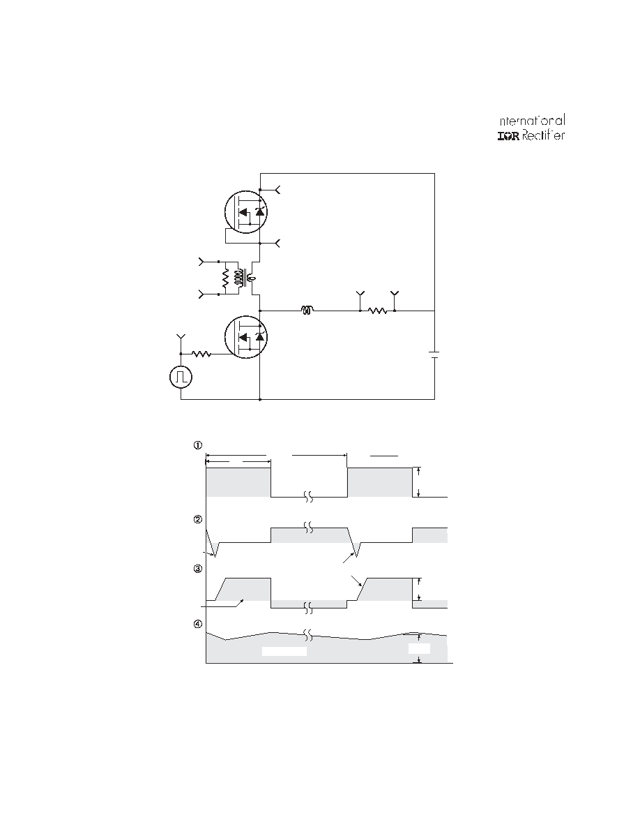
Peak Diode Recovery dv/dt Test Circuit
P.W.
Period
di/dt
Diode Recovery
dv/dt
Ripple
5%
Body Diode Forward Drop
Re-Applied
Voltage
Reverse
Recovery
Current
Body Diode Forward
Current
V
GS
=10V
V
DD
I
SD
Driver Gate Drive
D.U.T. I
SD
Waveform
D.U.T. V
DS
Waveform
Inductor Curent
D =
P.W.
Period
+
-
+
+
+
-
-
-
R
G
V
DD
· dv/dt controlled by R
G
· I
SD
controlled by Duty Factor "D"
· D.U.T. - Device Under Test
D.U.T
Circuit Layout Considerations
· Low Stray Inductance
· Ground Plane
· Low Leakage Inductance
Current Transformer
*
Reverse Polarity for P-Channel
** Use P-Channel Driver for P-Channel Measurements
*
V
GS
*
**
[ ]
[ ]
***
V
GS
= 5.0V for Logic Level and 3V Drive Devices
[ ] ***
Fig 13. For P-Channel HEXFETS
IRLML6302
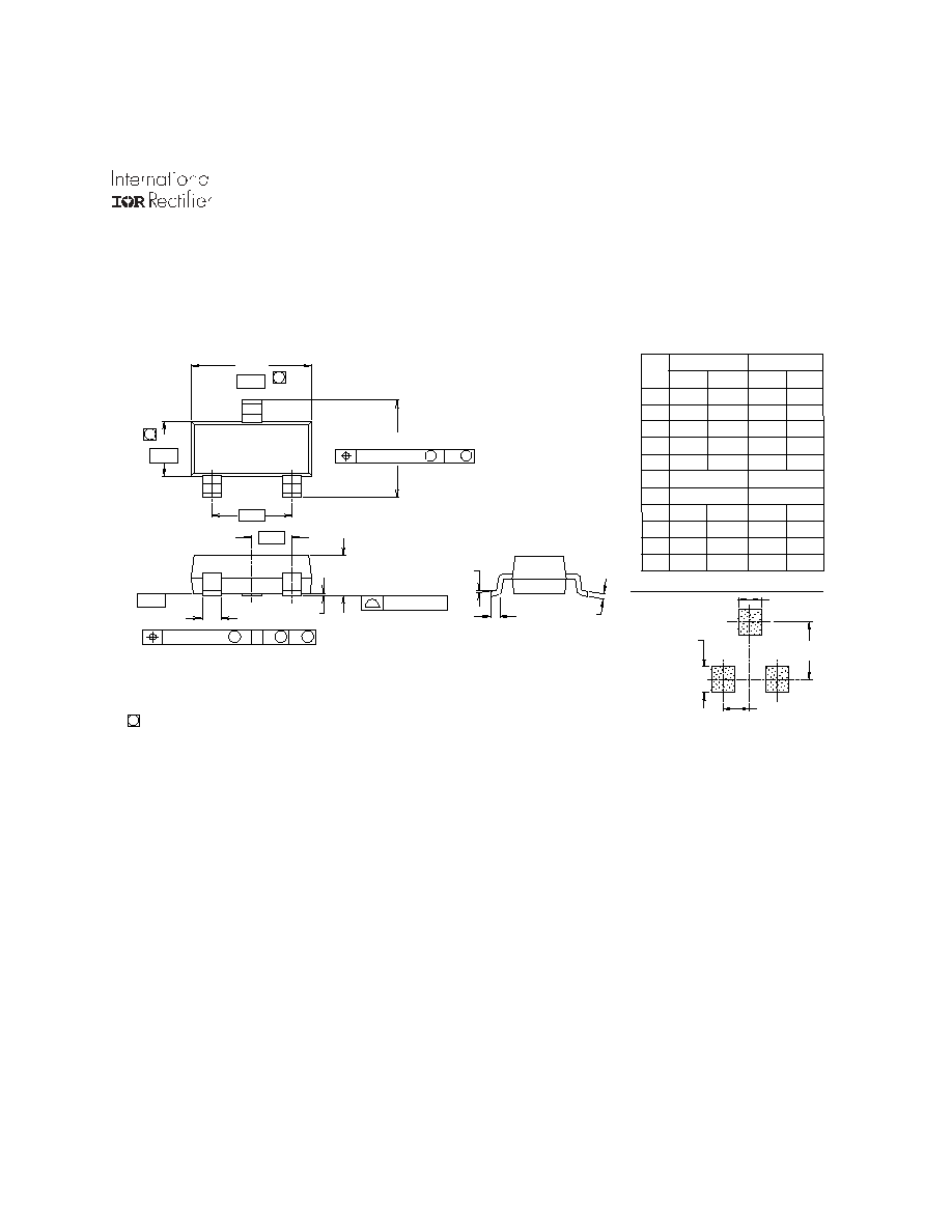
SOT-23 Outline
Dimensions are shown in millimeters (inches)
Package Outline
LEAD ASSIGNMENTS
1 - GATE
2 - SOURCE
3 - DRAIN
L
3X
3X
C
A1
- C -
B 3X
A
e
e1
0.008 (.003)
3
1
2
E
- A -
- B -
D
H
0.20 ( .008 ) M A M
DIM
INCHES MILLIMETERS
MIN MAX MIN MAX
A .032 .044 0.82 1.11
A1 .001 .004 0.02 0.10
B .015 .021 0.38 0.54
C .004 .006 0.10 0.15
D .105 .120 2.67 3.05
e .0750 BASIC 1.90 BASIC
e1 .0375 BASIC 0.95 BASIC
E .047 .055 1.20 1.40
H .083 .098 2.10 2.50
L .005 .010 0.13 0.25
0° 8° 0° 8°
0.10 (.004) M C A S B S
MINIMUM RECOMMENDED FOOTPRINT
0.80 ( .031 )
3X
2.00
( .079 )
0.95 ( .037 )
2X
0.90
( .035 )
3X
3
3
3
NOTES:
1. DIMENSIONING & TOLERANCING PER ANSI Y14.5M-1982.
2. CONTROLLING DIMENSION : INCH.
DIMENSIONS DO NOT INCLUDE MOLD FLASH.
IRLML6302
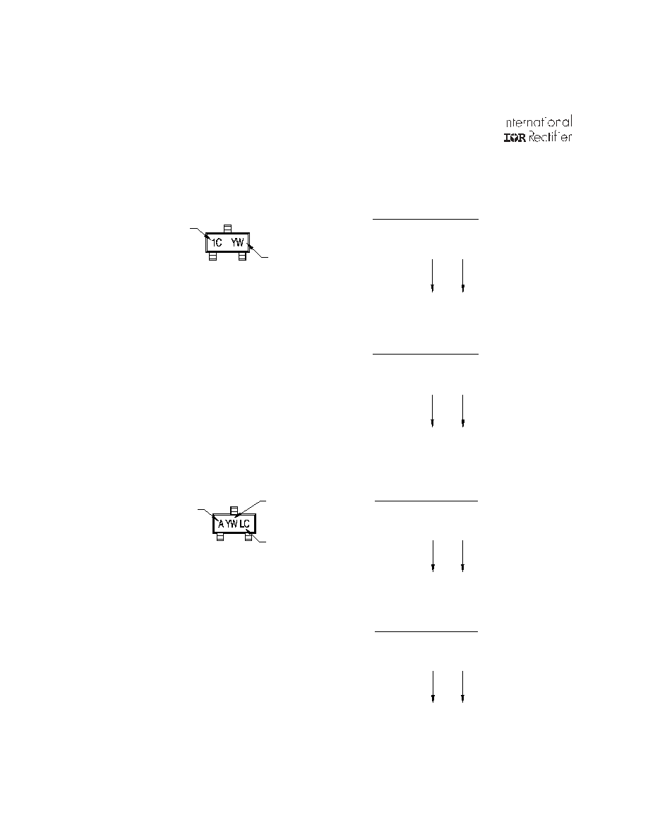
Part Marking Information
6
1996
26
24
25
30
28
WEEK
27
WORK
29
2002
2003
1995
1994
2001
YEAR
B
D
E
C
Y
A
2000
1997
1999
1998
0
8
9
7
D
C
W
B
A
X
Z
Y
04
WEEK
WORK
02
01
03
2002
2003
1995
1994
YEAR
2001
2
4
5
3
Y
1
W
D
C
B
A
EXAMPLE: THIS IS AN IRLML6302
DATE CODE EXAMPLES:
YWW = 9532 = EF
YWW = 9503 = 5C
WW = (1-26) IF PRECEDED BY LAS T DIGIT OF CALENDAR YEAR
Notes : This part marking information applies to devices produced before 02/26/2001
F
1996
52
51
50
2000
1997
1999
1998
K
H
J
G
X
Z
Y
PART NUMBER
PART NUMBER CODE REFERENCE:
WW = (27-52) IF PRECEDED BY A LETTER
DATE
1C = IRLML6302
1D = IRLML5103
1F = IRLML6401
1G = IRLML2502
1H = IRLML5203
1E = IRLML6402
1A = IRLML2402
1B = IRLML2803
CODE
SOT-23
29
30
50
W
YEAR
A
2001
A
B
2002
B
C
2003
C
D
1994
D
X
J
1995
1996
1997
1998
1999
2000
E
F
G
H
K
Y
1995
1996
1997
1998
2000
9
8
7
6
5
PART NUMBER
Y = YEAR
W = WEEK
WORK
WEEK
WORK
A = IRLML2402
B = IRLML2803
C = IRLML6302
D = IRLML5103
PART NUMBER CODE REFERENCE:
25
Y
51
Y
26
Z
52
Z
G = IRLML2502
F = IRLML6401
E = IRLML6402
H = IRLML5203
LOT
CODE
Notes: This part marking information applies to devices produced after 02/26/2001
W = (1-26) IF PRECEDED BY LAST DIGIT OF CALENDAR YEAR
01
02
03
04
24
W
YEAR
Y
A
2001
1
B
2002
2
C
2003
3
D
1994
4
X
1999
0
W = (27-52) IF PRECEDED BY A LETTER
WEEK
27
28
IRLML6302
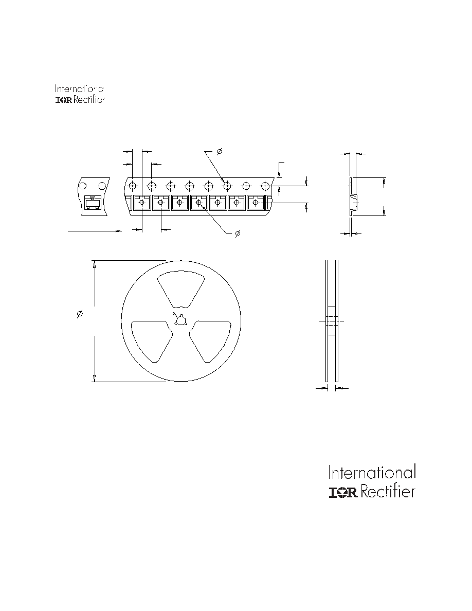
Tape & Reel Information
SOT-23
Dimensions are shown in millimeters (inches)
2.05 ( .080 )
1.95 ( .077 )
TR
FEED DIRECTION
4.1 ( .161 )
3.9 ( .154 )
1.6 ( .062 )
1.5 ( .060 )
1.85 ( .072 )
1.65 ( .065 )
3.55 ( .139 )
3.45 ( .136 )
1.1 ( .043 )
0.9 ( .036 )
4.1 ( .161 )
3.9 ( .154 )
0.35 ( .013 )
0.25 ( .010 )
8.3 ( .326 )
7.9 ( .312 )
1.32 ( .051 )
1.12 ( .045 )
9.90 ( .390 )
8.40 ( .331 )
178.00
( 7.008 )
MAX.
NOTES:
1. CONTROLLING DIMENSION : MILLIMETER.
2. OUTLINE CONFORMS TO EIA-481 & EIA-541.
Data and specifications subject to change without notice.
IR WORLD HEADQUARTERS: 233 Kansas St., El Segundo, California 90245, USA Tel: (310) 252-7105
TAC Fax: (310) 252-7903
Visit us at www.irf.com for sales contact information. 04/03