
IRLL024N
HEXFET
Û
Power MOSFET
PD - 91895
S
D
G
V
DSS
= 55V
R
DS(on)
= 0.065
I
D
= 3.1A
Fifth Generation HEXFETs from International Rectifier
utilize advanced processing techniques to achieve
extremely low on-resistance per silicon area. This benefit,
combined with the fast switching speed and ruggedized
device design that HEXFET Power MOSFETs are well
known for, provides the designer with an extremely efficient
and reliable device for use in a wide variety of applications.
The SOT-223 package is designed for surface-mount
using vapor phase, infra red, or wave soldering techniques.
Its unique package design allows for easy automatic pick-
and-place as with other SOT or SOIC packages but has
the added advantage of improved thermal performance
due to an enlarged tab for heatsinking. Power dissipation
of 1.0W is possible in a typical surface mount application.
6/15/99
Description
l
Surface Mount
l
Advanced Process Technology
l
Ultra Low On-Resistance
l
Dynamic dv/dt Rating
l
Fast Switching
l
Fully Avalanche Rated
S O T -2 2 3
* When mounted on FR-4 board using minimum recommended footprint.
** When mounted on 1 inch square copper board, for comparison with other SMD devices.
Parameter
Typ.
Max.
Units
R
JA
Junction-to-Amb. (PCB Mount, steady state)*
90
120
R
JA
Junction-to-Amb. (PCB Mount, steady state)**
50
60
Thermal Resistance
¯C/W
Parameter
Max.
Units
I
D
@ T
A
= 25¯C
Continuous Drain Current, V
GS
@ 10V**
4.4
I
D
@ T
A
= 25¯C
Continuous Drain Current, V
GS
@ 10V*
3.1
I
D
@ T
A
= 70¯C
Continuous Drain Current, V
GS
@ 10V*
2.5
I
DM
Pulsed Drain Current
12
P
D
@T
A
= 25¯C
Power Dissipation (PCB Mount)**
2.1
W
P
D
@T
A
= 25¯C
Power Dissipation (PCB Mount)*
1.0
W
Linear Derating Factor (PCB Mount)*
8.3
mW/¯C
V
GS
Gate-to-Source Voltage
Ý 16
V
E
AS
Single Pulse Avalanche Energy
120
mJ
I
AR
Avalanche Current
3.1
A
E
AR
Repetitive Avalanche Energy
*
0.1
mJ
dv/dt
Peak Diode Recovery dv/dt
5.0
V/ns
T
J,
T
STG
Junction and Storage Temperature Range
-55 to + 150
¯C
Absolute Maximum Ratings
A
www.irf.com
1

IRLL024N
2
www.irf.com
Parameter
Min. Typ. Max. Units
Conditions
V
(BR)DSS
Drain-to-Source Breakdown Voltage
55
ÙÙÙ
ÙÙÙ
V
V
GS
= 0V, I
D
= 250çA
V
(BR)DSS
/
T
J
Breakdown Voltage Temp. Coefficient
ÙÙÙ
0.048 ÙÙÙ
V/¯C
Reference to 25¯C, I
D
= 1mA
ÙÙÙ
ÙÙÙ 0.065
V
GS
= 10V, I
D
= 3.1A
ÙÙÙ
ÙÙÙ 0.080
V
GS
= 5.0V, I
D
= 2.5A
ÙÙÙ
ÙÙÙ 0.100
V
GS
= 4.0V, I
D
= 1.6A
V
GS(th)
Gate Threshold Voltage
1.0
ÙÙÙ
2.0
V
V
DS
= V
GS
, I
D
= 250çA
g
fs
Forward Transconductance
3.3
ÙÙÙ
ÙÙÙ
S
V
DS
= 25V, I
D
= 1.9 A
ÙÙÙ
ÙÙÙ
25
çA
V
DS
= 55V, V
GS
= 0V
ÙÙÙ
ÙÙÙ
250
V
DS
= 44V, V
GS
= 0V, T
J
= 125¯C
Gate-to-Source Forward Leakage
ÙÙÙ
ÙÙÙ
100
nA
V
GS
= 16V
Gate-to-Source Reverse Leakage
ÙÙÙ
ÙÙÙ
-100
V
GS
= -16V
Q
g
Total Gate Charge
ÙÙÙ
10.4 15.6
I
D
= 1.9A
Q
gs
Gate-to-Source Charge
ÙÙÙ
1.5
2.3
nC
V
DS
= 44V
Q
gd
Gate-to-Drain ("Miller") Charge
ÙÙÙ
5.5
8.3
V
GS
= 5.0V, See Fig. 6 and 9
t
d(on)
Turn-On Delay Time
ÙÙÙ
7.4
ÙÙÙ
V
DD
= 28V
t
r
Rise Time
ÙÙÙ
21
ÙÙÙ
ns
I
D
= 1.9A
t
d(off)
Turn-Off Delay Time
ÙÙÙ
18
ÙÙÙ
R
G
= 24
t
f
Fall Time
ÙÙÙ
25
ÙÙÙ
R
D
= 15
,
See Fig. 10
C
iss
Input Capacitance
ÙÙÙ
510
ÙÙÙ
V
GS
= 0V
C
oss
Output Capacitance
ÙÙÙ
140
ÙÙÙ
pF
V
DS
= 25V
C
rss
Reverse Transfer Capacitance
ÙÙÙ
58
ÙÙÙ
= 1.0MHz, See Fig. 5
Electrical Characteristics @ T
J
= 25¯C (unless otherwise specified)
I
GSS
R
DS(on)
Static Drain-to-Source On-Resistance
I
DSS
Drain-to-Source Leakage Current
Repetitive rating; pulse width limited by
max. junction temperature. ( See fig. 11 )
I
SD
1.9A, di/dt
270A/çs, V
DD
V
(BR)DSS
,
T
J
150¯C
Notes:
Starting T
J
= 25¯C, L = 25 mH
R
G
= 25
, I
AS
= 3.1A. (See Figure 12)
Pulse width
300çs; duty cycle
2%.
Parameter
Min. Typ. Max. Units
Conditions
I
S
Continuous Source Current
MOSFET symbol
(Body Diode)
showing the
I
SM
Pulsed Source Current
integral reverse
(Body Diode)
p-n junction diode.
V
SD
Diode Forward Voltage
ÙÙÙ
ÙÙÙ
1.0
V
T
J
= 25¯C, I
S
= 1.9A, V
GS
= 0V
t
rr
Reverse Recovery Time
ÙÙÙ
39
58
ns
T
J
= 25¯C, I
F
= 1.9A
Q
rr
Reverse RecoveryCharge
ÙÙÙ
63
94
nC
di/dt = 100A/çs
t
on
Forward Turn-On Time
Intrinsic turn-on time is negligible (turn-on is dominated by L
S
+L
D
)
Source-Drain Ratings and Characteristics
ÙÙÙ
ÙÙÙ
ÙÙÙ
ÙÙÙ
12
3.1
A

IRLL024N
www.irf.com
3
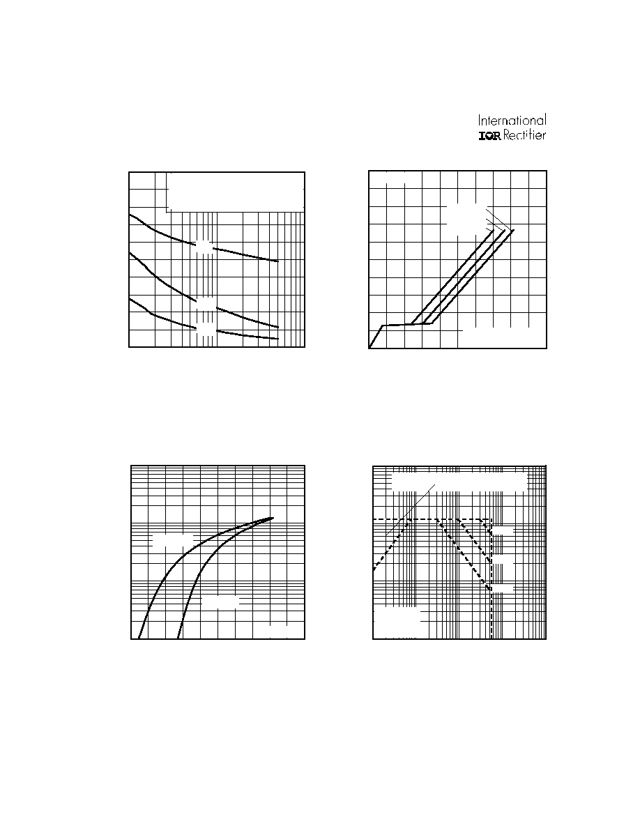
Fig 4. Normalized On-Resistance
Vs. Temperature
Fig 2. Typical Output Characteristics
Fig 1. Typical Output Characteristics
Fig 3. Typical Transfer Characteristics
1
10
100
0.1
1
10
100
20çs PULSE WIDTH
T = 25 C
J
¯
TOP
BOTTOM
VGS
15V
10V
7.0V
5.5V
4.5V
4.0V
3.5V
2.7V
V , Drain-to-Source Voltage (V)
I , Drain-to-Source Current (A)
DS
D
2.7V
1
10
100
0.1
1
10
100
20çs PULSE WIDTH
T = 150 C
J
¯
TOP
BOTTOM
VGS
15V
10V
7.0V
5.5V
4.5V
4.0V
3.5V
2.7V
V , Drain-to-Source Voltage (V)
I , Drain-to-Source Current (A)
DS
D
2.7V
-60 -40 -20
0
20
40
60
80 100 120 140 160
0.0
0.5
1.0
1.5
2.0
T , Junction Temperature ( C)
R , Drain-to-Source On Resistance
(Normalized)
J
DS(on)
¯
V
=
I =
GS
D
10V
3.1A
1
10
100
2
4
6
8
10
12
V = 25V
20çs PULSE WIDTH
DS
V , Gate-to-Source Voltage (V)
I , Drain-to-Source Current (A)
GS
D
T = 25 C
J
¯
T = 150 C
J
¯
IRLL024N
4
www.irf.com
Fig 8. Maximum Safe Operating Area
Fig 6. Typical Gate Charge Vs.
Gate-to-Source Voltage
Fig 5. Typical Capacitance Vs.
Drain-to-Source Voltage
Fig 7. Typical Source-Drain Diode
Forward Voltage
1
10
100
0
200
400
600
800
1000
V , Drain-to-Source Voltage (V)
C, Capacitance (pF)
DS
V
C
C
C
=
=
=
=
0V,
C
C
C
f = 1MHz
+ C
+ C
C SHORTED
GS
iss
gs
gd ,
ds
rss
gd
oss
ds
gd
Ciss
Coss
Crss
0
4
8
12
16
20
0
3
6
9
12
15
Q , Total Gate Charge (nC)
V , Gate-to-Source Voltage (V)
G
GS
FOR TEST CIRCUIT
SEE FIGURE
I =
D
13
1.9A
V
= 11V
DS
V
= 27V
DS
V
= 44V
DS
0.1
1
10
100
0.4
0.6
0.8
1.0
1.2
1.4
V ,Source-to-Drain Voltage (V)
I , Reverse Drain Current (A)
SD
SD
V = 0 V
GS
T = 25 C
J
¯
T = 150 C
J
¯
0.1
1
10
100
0.1
1
10
100
1000
OPERATION IN THIS AREA LIMITED
BY R
DS(on)
Single Pulse
T
T
= 150 C
= 25 C
¯
¯
J
C
V , Drain-to-Source Voltage (V)
I , Drain Current (A)
I , Drain Current (A)
DS
D
100us
1ms
10ms

IRLL024N
www.irf.com
5
Fig 11. Maximum Effective Transient Thermal Impedance, Junction-to-Ambient
Fig 9. Maximum Drain Current Vs.
Case Temperature
0.1
1
10
100
1000
0.00001
0.0001
0.001
0.01
0.1
1
10
100
Notes:
1. Duty factor D =
t / t
2. Peak T = P
x Z
+ T
1
2
J
DM
thJA
A
P
t
t
DM
1
2
t , Rectangular Pulse Duration (sec)
Thermal Response
(Z )
1
thJA
0.01
0.02
0.05
0.10
0.20
D = 0.50
SINGLE PULSE
(THERMAL RESPONSE)
25
50
75
100
125
150
0.0
1.0
2.0
3.0
4.0
T , Case Temperature
( C)
I , Drain Current (A)
¯
C
D
Fig 10a. Switching Time Test Circuit
V
DS
90%
10%
V
GS
t
d(on)
t
r
t
d(off)
t
f
Fig 10b. Switching Time Waveforms
V
DS
Pulse Width
1
çs
Duty Factor
0.1 %
R
D
V
GS
R
G
D.U.T.
5.0V
+
-
V
DD