Äîêóìåíòàöèÿ è îïèñàíèÿ www.docs.chipfind.ru
IRLI530N
PRELIMINARY
HEXFET
®
Power MOSFET
PD - 9.1350B
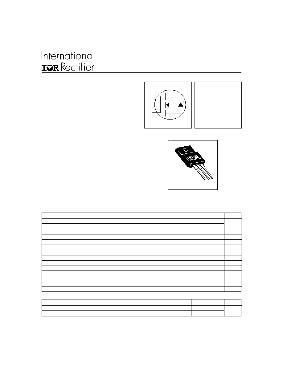
S
D
G
V
DSS
= 100V
R
DS(on)
= 0.10
I
D
= 12A
l
Logic-Level Gate Drive
l
Advanced Process Technology
l
Isolated Package
l
High Voltage Isolation = 2.5KVRMS
l
Sink to Lead Creepage Dist. = 4.8mm
l
Fully Avalanche Rated
TO-220 FULLPAK
3/16/98
Parameter
Typ.
Max.
Units
R
JC
Junction-to-Case
3.7
R
JA
Junction-to-Ambient
65
Thermal Resistance
Parameter
Max.
Units
I
D
@ T
C
= 25°C
Continuous Drain Current, V
GS
@ 10V
12
I
D
@ T
C
= 100°C
Continuous Drain Current, V
GS
@ 10V
8.6
A
I
DM
Pulsed Drain Current
60
P
D
@T
C
= 25°C
Power Dissipation
41
W
Linear Derating Factor
0.27
W/°C
V
GS
Gate-to-Source Voltage
± 16
V
E
AS
Single Pulse Avalanche Energy
150
mJ
I
AR
Avalanche Current
9.0
A
E
AR
Repetitive Avalanche Energy
4.1
mJ
dv/dt
Peak Diode Recovery dv/dt
5.0
V/ns
T
J
Operating Junction and
-55 to + 175
T
STG
Storage Temperature Range
Soldering Temperature, for 10 seconds
300 (1.6mm from case )
°C
Mounting torque, 6-32 or M3 screw
10 lbf·in (1.1N·m)
Absolute Maximum Ratings
°C/W
Description
Fifth Generation HEXFETs from International Rectifier
utilize advanced processing techniques to achieve
extremely low on-resistance per silicon area. This
benefit, combined with the fast switching speed and
ruggedized device design that HEXFET Power
MOSFETs are well known for, provides the designer
with an extremely efficient and reliable device for use
in a wide variety of applications.
The TO-220 Fullpak eliminates the need for additional
insulating hardware in commercial-industrial
applications. The moulding compound used provides
a high isolation capability and a low thermal resistance
between the tab and external heatsink. This isolation
is equivalent to using a 100 micron mica barrier with
standard TO-220 product. The Fullpak is mounted to
a heatsink using a single clip or by a single screw
fixing.
IRLI530N
Parameter
Min. Typ. Max. Units
Conditions
V
(BR)DSS
Drain-to-Source Breakdown Voltage
100
V
V
GS
= 0V, I
D
= 250µA
V
(BR)DSS
/
T
J
Breakdown Voltage Temp. Coefficient
0.122
V/°C
Reference to 25°C, I
D
= 1mA
0.100
V
GS
= 10V, I
D
= 9.0A
0.120
V
GS
= 5.0V, I
D
= 9.0A
0.150
V
GS
= 4.0V, I
D
= 8.0A
V
GS(th)
Gate Threshold Voltage
1.0
2.0
V
V
DS
= V
GS
, I
D
= 250µA
g
fs
Forward Transconductance
7.7
S
V
DS
= 50V, I
D
= 9.0A
25
µA
V
DS
= 100V, V
GS
= 0V
250
V
DS
= 80V, V
GS
= 0V, T
J
= 150°C
Gate-to-Source Forward Leakage
100
nA
V
GS
= 16V
Gate-to-Source Reverse Leakage
-100
V
GS
= -16V
Q
g
Total Gate Charge
34
I
D
= 9.0A
Q
gs
Gate-to-Source Charge
4.8
nC
V
DS
= 80V
Q
gd
Gate-to-Drain ("Miller") Charge
20
V
GS
= 5.0V, See Fig. 6 and 13
t
d(on)
Turn-On Delay Time
7.2
V
DD
= 50V
t
r
Rise Time
53
ns
I
D
= 9.0A
t
d(off)
Turn-Off Delay Time
30
R
G
= 6.0
,
V
GS
= 5.0V
t
f
Fall Time
26
R
D
= 5.5
,
See Fig. 10
Between lead,
6mm (0.25in.)
from package
and center of die contact
C
iss
Input Capacitance
800
V
GS
= 0V
C
oss
Output Capacitance
160
V
DS
= 25V
C
rss
Reverse Transfer Capacitance
90
= 1.0MHz, See Fig. 5
C
Drain to Sink Capacitance
12
= 1.0MHz
Electrical Characteristics @ T
J
= 25°C (unless otherwise specified)
I
GSS
I
DSS
Drain-to-Source Leakage Current
S
D
G
L
D
Internal Drain Inductance
4.5
L
S
Internal Source Inductance
7.5
R
DS(on)
Static Drain-to-Source On-Resistance
nH
pF
S
D
G
Notes:
Repetitive rating; pulse width limited by
max. junction temperature. ( See fig. 11 )
Starting T
J
= 25°C, L = 3.1mH
R
G
= 25
, I
AS
= 9.0A. (See Figure 12)
t=60s, =60Hz
I
SD
9.0A, di/dt
540A/µs, V
DD
V
(BR)DSS
,
T
J
175°C
Uses IRL530N data and test conditions
Pulse width
300µs; duty cycle
2%.
Parameter
Min. Typ. Max. Units
Conditions
I
S
Continuous Source Current
MOSFET symbol
(Body Diode)
showing the
I
SM
Pulsed Source Current
integral reverse
(Body Diode)
p-n junction diode.
V
SD
Diode Forward Voltage
1.3
V
T
J
= 25°C, I
S
= 6.6A, V
GS
= 0V
t
rr
Reverse Recovery Time
140
210
ns
T
J
= 25°C, I
F
= 9.0A
Q
rr
Reverse RecoveryCharge
740 1100
nC
di/dt = 100A/µs
t
on
Forward Turn-On Time
Intrinsic turn-on time is negligible (turn-on is dominated by L
S
+L
D
)
Source-Drain Ratings and Characteristics
A
12
60
IRLI530N
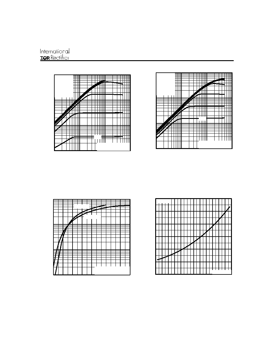
Fig 4. Normalized On-Resistance
Vs. Temperature
Fig 2. Typical Output Characteristics,
Fig 1. Typical Output Characteristics,
Fig 3. Typical Transfer Characteristics
0.1
1
10
1 00
0.1
1
1 0
100
I , D
r
a
i
n
-
to
-
S
o
u
r
c
e
C
u
r
r
e
n
t
(
A
)
D
V , D ra in-to-S ourc e V oltage (V )
D S
A
2 0 µ s P U L S E W ID T H
T = 2 5 °C
J
VGS
TOP 15V
12V
10V
8.0V
6.0V
4.0V
3.0V
BOTTOM 2.5V
2 .5 V
0.1
1
1 0
10 0
0.1
1
10
10 0
I , D
r
a
i
n
-
to
-
S
o
u
r
c
e
C
u
r
r
e
n
t
(
A
)
D
V , D rain-to-S ourc e V oltage (V )
D S
A
2 0 µ s P U L S E W ID T H
T = 1 7 5 °C
VGS
TOP 15V
12V
10V
8.0V
6.0V
4.0V
3.0V
BOTTOM 2.5V
2 .5 V
J
0.1
1
1 0
1 0 0
2
3
4
5
6
7
8
9
1 0
T = 2 5 °C
J
G S
V , G a te -to -S o u rc e V o lta g e (V )
D
I
,
D
r
ai
n-
t
o
-
S
ou
r
c
e C
u
r
r
e
n
t
(
A
)
V = 5 0 V
2 0 µ s P U L S E W ID T H
T = 1 7 5 °C
J
A
D S
0.0
0.5
1.0
1.5
2.0
2.5
3.0
-60
-40
-20
0
2 0
4 0
6 0
8 0
1 0 0 1 2 0 1 4 0 1 6 0 1 8 0
J
T , J unc tion T em perature (°C )
R
, D
r
a
i
n
-
to
-S
o
u
r
c
e
O
n
R
e
s
i
s
t
a
n
c
e
DS
(
o
n
)
(N
o
r
m
a
l
i
z
e
d
)
V = 1 0 V
G S
A
I = 1 5 A
D
IRLI530N
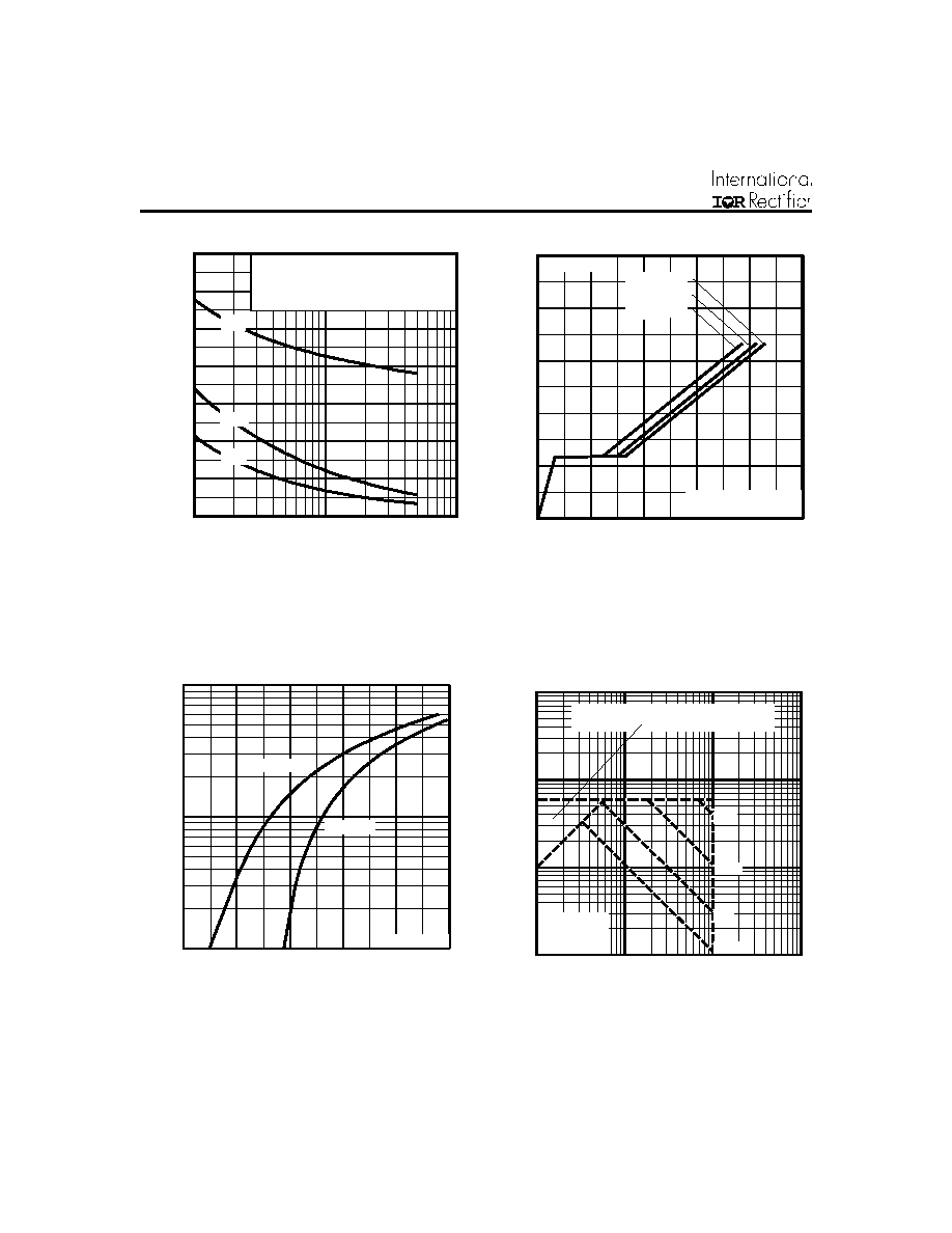
Fig 6. Typical Gate Charge Vs.
Gate-to-Source Voltage
Fig 8. Maximum Safe Operating Area
Fig 5. Typical Capacitance Vs.
Drain-to-Source Voltage
Fig 7. Typical Source-Drain Diode
Forward Voltage
0
2 00
4 00
6 00
8 00
1 0 00
1 2 00
1 4 00
1
10
1 0 0
C
,
C
apaci
t
a
n
c
e
(
p
F
)
D S
V , D rain-to -S ourc e V oltage (V )
A
V = 0 V , f = 1 M H z
C = C + C , C S H O R TE D
C = C
C = C + C
G S
iss g s gd ds
rss g d
o ss ds g d
C
is s
C
o s s
C
rs s
0
3
6
9
12
15
0
1 0
2 0
30
40
50
Q , Tota l G ate C h arg e (n C )
G
V
, G
a
te
-
t
o
-
S
o
u
r
c
e
V
o
lta
g
e
(
V
)
GS
V = 8 0 V
V = 5 0 V
V = 2 0 V
D S
D S
D S
A
F O R TE S T C IR C U IT
S E E F IG U R E 1 3
I = 9 .0 A
D
1
1 0
1 0 0
0.4
0.6
0.8
1.0
1.2
1.4
T = 2 5 °C
J
V = 0 V
G S
V , S o urc e-to -D rain V o lta ge (V )
I
,
R
e
v
e
r
s
e D
r
ai
n C
u
r
r
ent
(
A
)
S D
SD
A
T = 1 7 5 °C
J
1
10
1 0 0
1 0 0 0
1
1 0
1 00
1000
V , D ra in-to-S o urc e V o lta ge (V )
D S
I
,
D
r
ai
n C
u
r
r
e
nt
(
A
)
O P E R A TIO N IN T H IS A R E A L IM ITE D
B Y R
D
D S (on)
10µ s
10 0µ s
1m s
1 0m s
A
T = 2 5 °C
T = 1 7 5 °C
S in g le P u ls e
C
J
IRLI530N
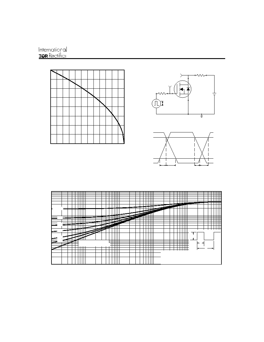
Fig 10a. Switching Time Test Circuit
V
DS
90%
10%
V
GS
t
d(on)
t
r
t
d(off)
t
f
Fig 10b. Switching Time Waveforms
V
DS
Pulse Width
1
µs
Duty Factor
0.1 %
R
D
V
GS
R
G
D.U.T.
5.0V
+
-
V
DD
Fig 11. Maximum Effective Transient Thermal Impedance, Junction-to-Case
Fig 9. Maximum Drain Current Vs.
Case Temperature
0.01
0.1
1
10
0.00001
0.0001
0.001
0.01
0.1
1
Notes:
1. Duty factor D = t / t
2. Peak T = P
x Z
+ T
1
2
J
DM
thJC
C
P
t
t
DM
1
2
t , Rectangular Pulse Duration (sec)
Thermal Response
(Z )
1
thJC
0.01
0.02
0.05
0.10
0.20
D = 0.50
SINGLE PULSE
(THERMAL RESPONSE)
25
50
75
100
125
150
175
0
3
6
9
12
T , Case Temperature ( C)
I , Drain Current (A)
°
C
D