IRLBA3803.p65
IRLBA3803
HEXFET
®
Power MOSFET
Logic-Level Gate Drive
Advanced Process Technology
175°C Operating Temperature
Fast Switching
Fully Avalanche Rated
Purchase IRLBA3803/P for solder plated option.
Fifth Generation HEXFETs from International Rectifier utilize advanced processing
techniques to achieve extremely low on-resistance per silicon area. This benefit,
combined with the fast switching speed and ruggedized device design that HEXFET
Power MOSFETs are well known for, provides the designer with an extremely
efficient and reliable device for use in a wide variety of applications.
The Super-220 is a package that has been designed to have the same mechanical
outline and pinout as the industry standard TO-220 but can house a considerably
larger silicon die. It has increased current handling capability over both the TO-220
and the much larger TO-247 package. This makes it ideal to reduce component
count in multiparalled TO-220 applications, reduce system power dissipation,
upgrade existing designs or have TO-247 performance in a TO-220 outline.
This package has also been designed to meet automotive qualification standard
Q101.
Description
V
DSS
= 30V
R
DS(on)
= 0.005
I
D
= 179A
V
S
D
G
05/20/02
www.irf.com
1
Absolute Maximum Ratings
Parameter
Typ.
Max.
Units
R
JC
Junction-to-Case
0.55
R
CS
Case-to-Sink, Flat, Greased Surface
0.5
°C/W
R
JA
Junction-to-Ambient
58
Thermal Resistance
Super - 220
Parameter
Max.
Units
I
D
@ T
C
= 25°C
Continuous Drain Current, V
GS
@ 10V
179
V
I
D
@ T
C
= 100°C
Continuous Drain Current, V
GS
@ 10V
126
V
A
I
DM
Pulsed Drain Current
Q
720
P
D
@T
C
= 25°C
Power Dissipation
270
W
Linear Derating Factor
1.8
W/°C
V
GS
Gate-to-Source Voltage
±16
V
E
AS
Single Pulse Avalanche Energy
RU
610
mJ
I
AR
Avalanche Current
QU
71
A
E
AR
Repetitive Avalanche Energy
Q
27
mJ
dv/dt
Peak Diode Recovery dv/dt
SU
5.0
V/ns
T
J
Operating Junction and
-55 to + 175
T
STG
Storage Temperature Range
Soldering Temperature, for 10 seconds
300 (1.6mm from case )
Recommended clip force
20
N
°C
PD - 91841C
IRLBA3803
2
www.irf.com
Parameter
Min. Typ. Max. Units
Conditions
I
S
Continuous Source Current
MOSFET symbol
(Body Diode)
showing the
I
SM
Pulsed Source Current
integral reverse
(Body Diode)
Q
p-n junction diode.
V
SD
Diode Forward Voltage
1.3
V
T
J
= 25°C, I
S
= 71A, V
GS
= 0V
T
t
rr
Reverse Recovery Time
120
180
ns
T
J
= 25°C, I
F
= 71A
Q
r r
Reverse Recovery Charge
450
680
nC
di/dt = 100A/µs
TU
t
on
Forward Turn-On Time
Intrinsic turn-on time is negligible (turn-on is dominated by L
S
+L
D
)
Q
Repetitive rating; pulse width limited by
max. junction temperature. ( See fig. 11 )
S
I
SD
71A, di/dt
130A/µs, V
DD
V
(BR)DSS
,
T
J
175°C
Notes:
R
V
DD
= 15V, starting T
J
= 25°C, L = 180µH
R
G
= 25
, I
AS
= 71A. (See Figure 12)
T
Pulse width
300µs; duty cycle
2%.
U
Uses IRL3803 data and test conditions.
Source-Drain Ratings and Characteristics
A
179
V
720
S
D
G
V
Calculated continuous current based on maximum allowable
junction temperature;for recommended current-handling of the
package refer to Design Tip # 93-4
Parameter
Min. Typ. Max. Units
Conditions
V
(BR)DSS
Drain-to-Source Breakdown Voltage
30
V
V
GS
= 0V, I
D
= 250µA
V
(BR)DSS
/
T
J
Breakdown Voltage Temp. Coefficient
0.052
V/°C
Reference to 25°C, I
D
= 1mA
U
0.005
V
GS
= 10V, I
D
= 71A
T
0.009
V
GS
= 4.5V, I
D
= 59A
T
V
GS(th)
Gate Threshold Voltage
1.0
V
V
DS
= V
GS
, I
D
= 250µA
g
fs
Forward Transconductance
55
S
V
DS
= 25V, I
D
= 71A
U
25
µA
V
DS
= 30V, V
GS
= 0V
250
V
DS
= 24V, V
GS
= 0V, T
J
= 150°C
Gate-to-Source Forward Leakage
100
V
GS
= 16V
Gate-to-Source Reverse Leakage
-100
nA
V
GS
= -16V
Q
g
Total Gate Charge
140
I
D
= 71A
Q
gs
Gate-to-Source Charge
41
nC
V
DS
= 24V
Q
gd
Gate-to-Drain ("Miller") Charge
78
V
GS
= 4.5V, See Fig. 6 and 13
TU
t
d(on)
Turn-On Delay Time
14
V
DD
= 15V
t
r
Rise Time
230
I
D
= 71A
t
d(off)
Turn-Off Delay Time
29
R
G
= 1.3
t
f
Fall Time
35
R
D
= 0.20
, See Fig. 10
TU
Between lead,
6mm (0.25in.)
from package
and center of die contact
C
iss
Input Capacitance
5000
V
GS
= 0V
C
oss
Output Capacitance
1800
pF
V
DS
= 25V
C
rss
Reverse Transfer Capacitance
880
= 1.0MHz, See Fig. 5
U
Electrical Characteristics @ T
J
= 25°C (unless otherwise specified)
nH
I
GSS
S
D
G
L
S
Internal Source Inductance
5.0
R
DS(on)
Static Drain-to-Source On-Resistance
L
D
Internal Drain Inductance
2.0
I
DSS
Drain-to-Source Leakage Current
IRLBA3803
www.irf.com
3
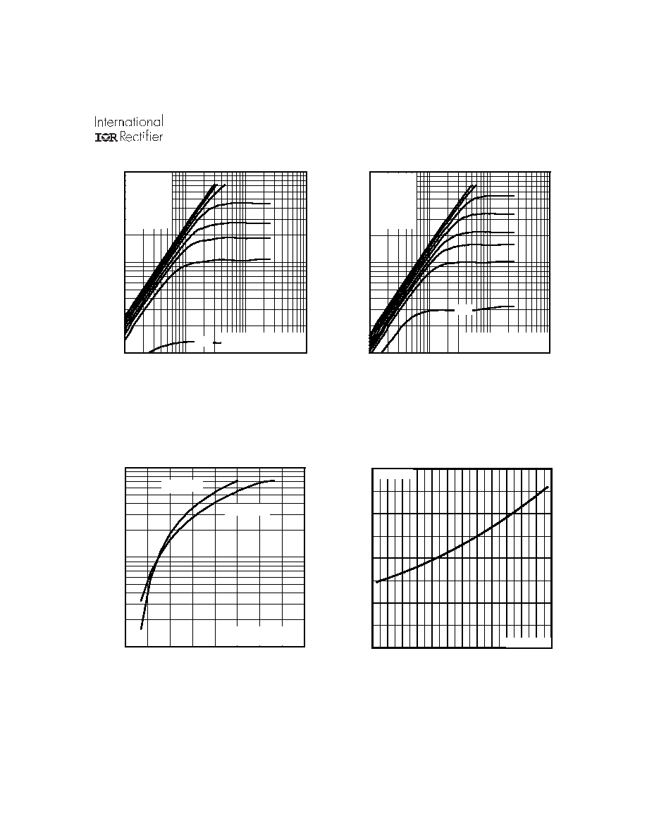
Fig 1. Typical Output Characteristics
Fig 3. Typical Transfer Characteristics
Fig 4. Normalized On-Resistance
Vs. Temperature
Fig 2. Typical Output Characteristics
0 . 0
0 . 5
1 . 0
1 . 5
2 . 0
- 6 0
- 4 0
- 2 0
0
2 0
4 0
6 0
8 0
1 0 0 1 2 0 1 4 0 1 6 0 1 8 0
J
T , Junction T em perature (°C )
R
, D
r
a
i
n
-
to
-
S
o
u
r
c
e
O
n
R
e
s
i
s
t
a
n
c
e
DS
(
o
n
)
(
N
or
m
a
l
i
z
ed)
V = 10 V
G S
A
I = 1 20 A
D
10
100
1000
0.1
1
10
100
20µs PULSE WIDTH
T = 25 C
J
°
TOP
BOTTOM
VGS
15V
10V
7.0V
5.5V
4.5V
4.0V
3.5V
2.7V
V , Drain-to-Source Voltage (V)
I , Drain-to-Source Current (A)
DS
D
2.7V
10
100
1000
0.1
1
10
100
20µs PULSE WIDTH
T = 175 C
J
°
TOP
BOTTOM
VGS
15V
10V
7.0V
5.5V
4.5V
4.0V
3.5V
2.7V
V , Drain-to-Source Voltage (V)
I , Drain-to-Source Current (A)
DS
D
2.7V
10
100
1000
2.0
4.0
6.0
8.0
10.0
V = 25V
20µs PULSE WIDTH
DS
V , Gate-to-Source Voltage (V)
I , Drain-to-Source Current (A)
GS
D
T = 25 C
J
°
T = 175 C
J
°
IRLBA3803
4
www.irf.com
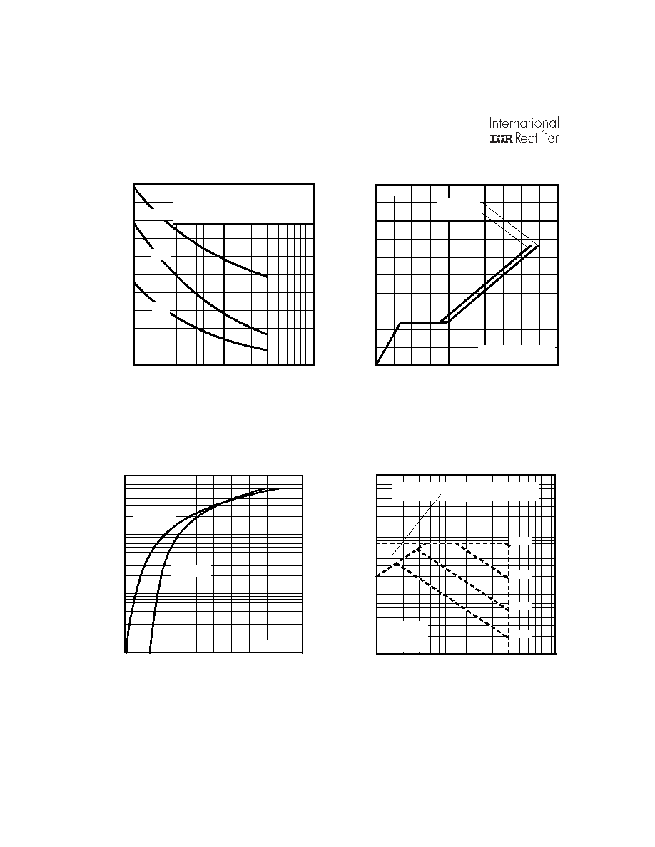
Fig 5. Typical Capacitance Vs.
Drain-to-Source Voltage
Fig 8. Maximum Safe Operating Area
Fig 6. Typical Gate Charge Vs.
Gate-to-Source Voltage
0
3
6
9
1 2
1 5
0
4 0
8 0
1 2 0
1 6 0
2 0 0
Q , T otal G ate C harge (nC )
G
V
, G
a
te
-
t
o
-
S
o
u
r
c
e
V
o
l
t
a
g
e
(
V
)
GS
A
F O R T E S T C IR C U IT
S E E F IG U R E 1 3
V = 24 V
V = 15 V
I = 71 A
D S
D S
D
0
2 0 0 0
4 0 0 0
6 0 0 0
8 0 0 0
1 0 0 0 0
1
1 0
1 0 0
C
,
C
a
pa
c
i
t
a
n
c
e (
p
F
)
D S
V , D rain-to-S ourc e V oltage (V )
A
V = 0V , f = 1 M H z
C = C + C , C S H O R TE D
C = C
C = C + C
G S
iss g s g d d s
rs s g d
o ss ds g d
C
is s
C
os s
C
rs s
Fig 7. Typical Source-Drain Diode
Forward Voltage
10
100
1000
10000
1
10
100
OPERATION IN THIS AREA LIMITED
BY R
DS(on)
Single Pulse
T
T
= 175 C
= 25 C
°
°
J
C
V , Drain-to-Source Voltage (V)
I , Drain Current (A)
I , Drain Current (A)
DS
D
10us
100us
1ms
10ms
1
10
100
1000
0.4
0.8
1.2
1.6
2.0
2.4
V ,Source-to-Drain Voltage (V)
I , Reverse Drain Current (A)
SD
SD
V = 0 V
GS
T = 25 C
J
°
T = 175 C
J
°
IRLBA3803
www.irf.com
5
Fig 9. Maximum Drain Current Vs.
Case Temperature
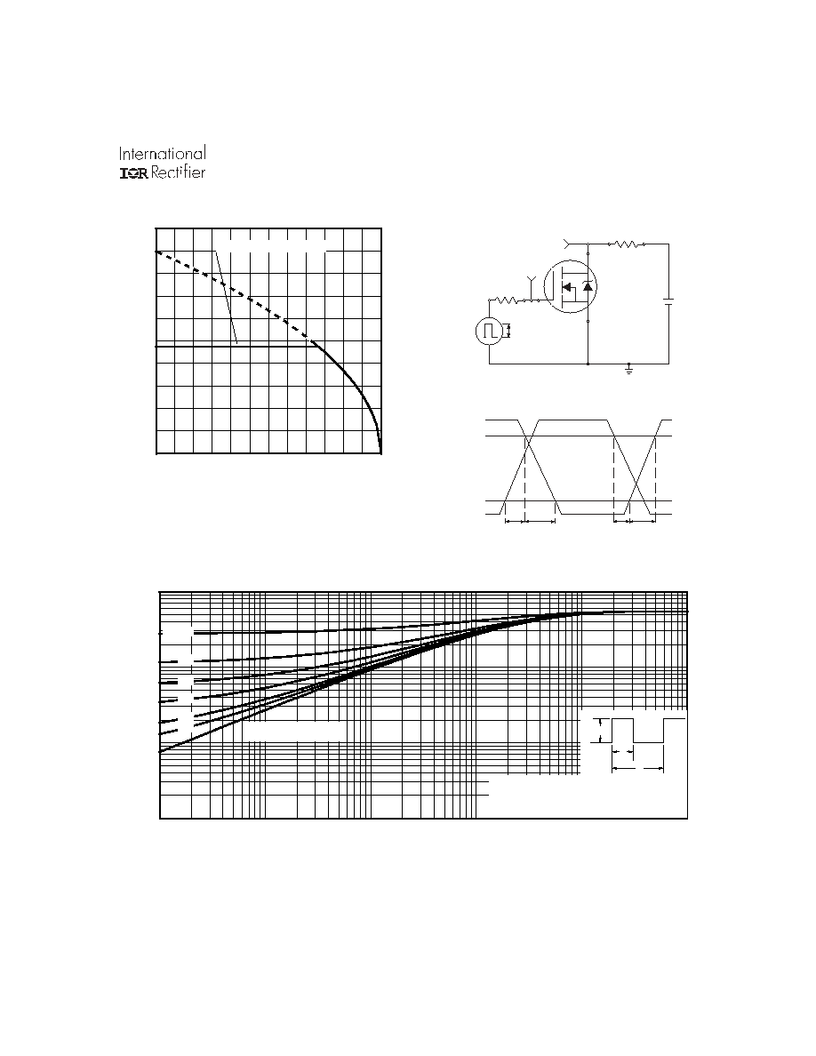
Fig 10a. Switching Time Test Circuit
V
DS
90%
10%
V
GS
t
d(on)
t
r
t
d(off)
t
f
Fig 10b. Switching Time Waveforms
Fig 11. Maximum Effective Transient Thermal Impedance, Junction-to-Case
V
DS
Pulse Width
1
µs
Duty Factor
0.1 %
R
D
V
GS
R
G
D.U.T.
4.5V
+
-
V
DD
0.001
0.01
0.1
1
0.00001
0.0001
0.001
0.01
0.1
1
Notes:
1. Duty factor D =
t / t
2. Peak T = P
x Z
+ T
1
2
J
DM
thJC
C
P
t
t
DM
1
2
t , Rectangular Pulse Duration (sec)
Thermal Response
(Z )
1
thJC
0.01
0.02
0.05
0.10
0.20
D = 0.50
SINGLE PULSE
(THERMAL RESPONSE)
25
50
75
100
125
150
175
0
40
80
120
160
200
T , Case Temperature ( C)
I , Drain Current (A)
°
C
D
LIMITED BY PACKAGE