IRL3103S
IRL3103L
HEXFET
®
Power MOSFET
02/14/02
Parameter
Typ.
Max.
Units
R
JC
Junction-to-Case
1.6
R
JA
Junction-to-Ambient (PCB mount)**
40
Thermal Resistance
www.irf.com
1
V
DSS
= 30V
R
DS(on)
= 12m
I
D
= 64A
S
D
G
Absolute Maximum Ratings
Parameter
Max.
Units
I
D
@ T
C
= 25°C
Continuous Drain Current, V
GS
@ 10V
64
I
D
@ T
C
= 100°C
Continuous Drain Current, V
GS
@ 10V
45
A
I
DM
Pulsed Drain Current
220
P
D
@T
C
= 25°C
Power Dissipation
94
W
Linear Derating Factor
0.63
W/°C
V
GS
Gate-to-Source Voltage
± 16
V
I
AR
Avalanche Current
34
A
E
AR
Repetitive Avalanche Energy
22
mJ
dv/dt
Peak Diode Recovery dv/dt
5.0
V/ns
T
J
Operating Junction and
-55 to + 175
T
STG
Storage Temperature Range
Soldering Temperature, for 10 seconds
300 (1.6mm from case )
°C
Mounting torque, 6-32 or M3 srew
10 lbf·in (1.1N·m)
Advanced HEXFET
®
Power MOSFETs from International
Rectifier utilize advanced processing techniques to
achieve extremely low on-resistance per silicon area.
This benefit, combined with the fast switching speed and
ruggedized device design that HEXFET power MOSFETs
are well known for, provides the designer with an
extremely efficient and reliable device for use in a wide
variety of applications.
The D
2
Pak is a surface mount power package capable of
accommodating die sizes up to HEX-4. It provides the
highest power capability and the lowest possible on-
resistance in any existing surface mount package. The
D
2
Pak is suitable for high current applications because of its
low internal connection resistance and can dissipate up to
2.0W in a typical surface mount application.
The through-hole version (IRL3103L) is available for low-
profile applications.
l
Advanced Process Technology
l
Surface Mount (IRL3103S)
l
Low-profile through-hole (IRL3103L)
l
175°C Operating Temperature
l
Fast Switching
l
Fully Avalanche Rated
Description
D
2
Pak
IRL3103S
TO-262
IRL3103L
°C/W
PD - 94162
IRL3103S/IRL3103L
2
www.irf.com
S
D
G
Parameter
Min. Typ. Max. Units
Conditions
I
S
Continuous Source Current
MOSFET symbol
(Body Diode)
showing the
I
SM
Pulsed Source Current
integral reverse
(Body Diode)
p-n junction diode.
V
SD
Diode Forward Voltage
1.2
V
T
J
= 25°C, I
S
= 34A, V
GS
= 0V
t
rr
Reverse Recovery Time
57
86
ns
T
J
= 25°C, I
F
= 34A
Q
rr
Reverse Recovery Charge
110
170
nC
di/dt = 100A/µs
t
on
Forward Turn-On Time
Intrinsic turn-on time is negligible (turn-on is dominated by L
S
+L
D
)
Source-Drain Ratings and Characteristics
64
220
A
Starting T
J
= 25°C, L = 220µH
R
G
= 25
, I
AS
= 34A, V
GS
=10V (See Figure 12)
Repetitive rating; pulse width limited by
max. junction temperature. (See fig. 11)
Notes:
I
SD
34A, di/dt
120A/µs, V
DD
V
(BR)DSS
,
T
J
175°C
Pulse width
400µs; duty cycle
2%.
This is a typical value at device destruction and represents
operation outside rated limits.
This is a calculated value limited to T
J
= 175°C .
**When mounted on 1" square PCB (FR-4 or G-10 Material). For
recommended footprint and soldering techniques refer to
application note #AN-994
Parameter
Min. Typ. Max. Units
Conditions
V
(BR)DSS
Drain-to-Source Breakdown Voltage
30
V
V
GS
= 0V, I
D
= 250µA
V
(BR)DSS
/
T
J
Breakdown Voltage Temp. Coefficient
0.028
V/°C
Reference to 25°C, I
D
= 1mA
12
V
GS
= 10V, I
D
= 34A
16
V
GS
= 4.5V, I
D
= 28A
V
GS(th)
Gate Threshold Voltage
1.0
V
V
DS
= V
GS
, I
D
= 250µA
g
fs
Forward Transconductance
22
S
V
DS
= 25V, I
D
= 34A
25
µA
V
DS
= 30V, V
GS
= 0V
250
V
DS
= 24V, V
GS
= 0V, T
J
= 150°C
Gate-to-Source Forward Leakage
100
V
GS
= 16V
Gate-to-Source Reverse Leakage
-100
nA
V
GS
= -16V
Q
g
Total Gate Charge
33
I
D
= 34A
Q
gs
Gate-to-Source Charge
5.9
nC
V
DS
= 24V
Q
gd
Gate-to-Drain ("Miller") Charge
17
V
GS
= 4.5V, See Fig. 6 and 13
t
d(on)
Turn-On Delay Time
8.9
V
DD
= 15V
t
r
Rise Time
120
I
D
= 34A
t
d(off)
Turn-Off Delay Time
14
R
G
= 1.8
t
f
Fall Time
9.1
V
GS
= 4.5V, See Fig. 10
Between lead,
6mm (0.25in.)
from package
and center of die contact
C
iss
Input Capacitance
1650
V
GS
= 0V
C
oss
Output Capacitance
650
V
DS
= 25V
C
rss
Reverse Transfer Capacitance
110
pF
= 1.0MHz, See Fig. 5
E
AS
Single Pulse Avalanche Energy
1320
130
mJ
I
AS
= 34A, L = 0.22mH
S
D
G
Electrical Characteristics @ T
J
= 25°C (unless otherwise specified)
R
DS(on)
Static Drain-to-Source On-Resistance
I
GSS
nH
L
S
Internal Source Inductance
7.5
L
D
Internal Drain Inductance
4.5
I
DSS
Drain-to-Source Leakage Current
m
IRL3103S/IRL3103L
www.irf.com
3
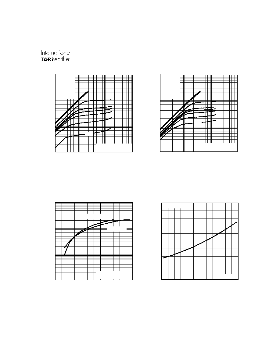
Fig 4. Normalized On-Resistance
Vs. Temperature
Fig 2. Typical Output Characteristics
Fig 1. Typical Output Characteristics
Fig 3. Typical Transfer Characteristics
1
10
100
1000
0.1
1
10
100
20µs PULSE WIDTH
T = 25 C
J
°
TOP
BOTTOM
VGS
15V
10V
4.5V
3.7V
3.5V
3.3V
3.0V
2.7V
V , Drain-to-Source Voltage (V)
I , Drain-to-Source Current (A)
DS
D
2.7V
1
10
100
1000
0.1
1
10
100
20µs PULSE WIDTH
T = 175 C
J
°
TOP
BOTTOM
VGS
15V
10V
4.5V
3.7V
3.5V
3.3V
3.0V
2.7V
V , Drain-to-Source Voltage (V)
I , Drain-to-Source Current (A)
DS
D
2.7V
1
10
100
1000
2.0
3.0
4.0
5.0
6.0
7.0
8.0
V = 15V
20µs PULSE WIDTH
DS
V , Gate-to-Source Voltage (V)
I , Drain-to-Source Current (A)
GS
D
T = 25 C
J
°
T = 175 C
J
°
-60 -40 -20
0
20 40 60 80 100 120 140 160 180
0.0
0.5
1.0
1.5
2.0
2.5
T , Junction Temperature ( C)
R , Drain-to-Source On Resistance
(Normalized)
J
DS(on)
°
V
=
I =
GS
D
10V
56A
IRL3103S/IRL3103L
4
www.irf.com
Fig 8. Maximum Safe Operating Area
Fig 6. Typical Gate Charge Vs.
Gate-to-Source Voltage
Fig 5. Typical Capacitance Vs.
Drain-to-Source Voltage
Fig 7. Typical Source-Drain Diode
Forward Voltage
1
10
100
0
500
1000
1500
2000
2500
3000
V , Drain-to-Source Voltage (V)
C, Capacitance (pF)
DS
V
C
C
C
=
=
=
=
0V,
C
C
C
f = 1MHz
+ C
+ C
C SHORTED
GS
iss
gs
gd ,
ds
rss
gd
oss
ds
gd
Ciss
Coss
Crss
0
10
20
30
40
0
3
6
9
12
15
Q , Total Gate Charge (nC)
V , Gate-to-Source Voltage (V)
G
GS
FOR TEST CIRCUIT
SEE FIGURE
I =
D
13
34A
V
= 15V
DS
V
= 24V
DS
0.1
1
10
100
1000
0.0
0.4
0.8
1.2
1.6
2.0
2.4
V ,Source-to-Drain Voltage (V)
I , Reverse Drain Current (A)
SD
SD
V = 0 V
GS
T = 25 C
J
°
T = 175 C
J
°
1
10
100
VDS , Drain-toSource Voltage (V)
1
10
100
1000
I D
, Drain-to-Source Current (A)
Tc = 25°C
Tj = 175°C
Single Pulse
1msec
10msec
OPERATION IN THIS AREA
LIMITED BY R DS(on)
100µsec
IRL3103S/IRL3103L
www.irf.com
5
Fig 11. Maximum Effective Transient Thermal Impedance, Junction-to-Case
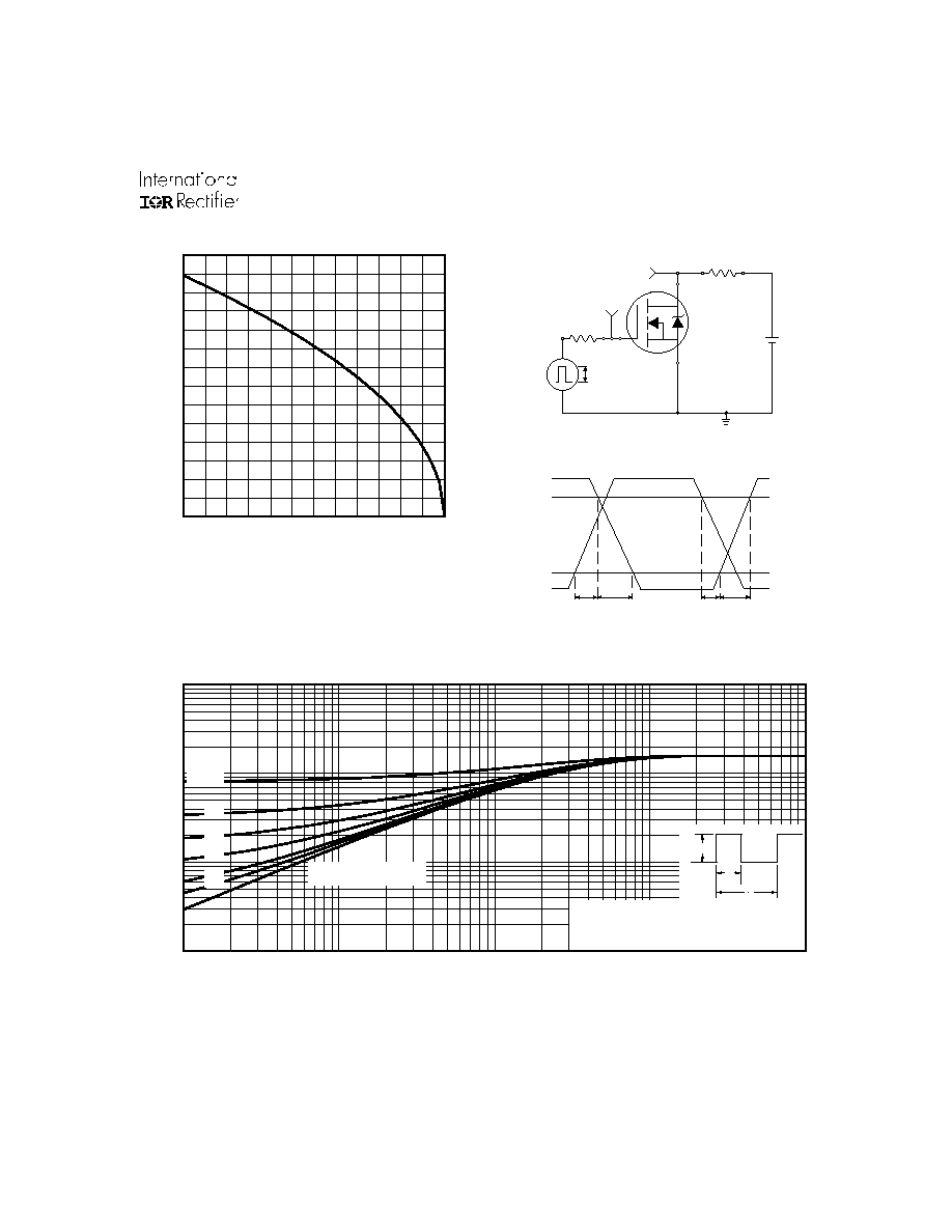
Fig 9. Maximum Drain Current Vs.
Case Temperature
0.01
0.1
1
10
0.00001
0.0001
0.001
0.01
0.1
Notes:
1. Duty factor D =
t / t
2. Peak T = P
x Z
+ T
1
2
J
DM
thJC
C
P
t
t
DM
1
2
t , Rectangular Pulse Duration (sec)
Thermal Response
(Z )
1
thJC
0.01
0.02
0.05
0.10
0.20
D = 0.50
SINGLE PULSE
(THERMAL RESPONSE)
25
50
75
100
125
150
175
0
10
20
30
40
50
60
70
T , Case Temperature
( C)
I , Drain Current (A)
°
C
D
V
DS
90%
10%
V
GS
t
d(on)
t
r
t
d(off)
t
f
V
DS
Pulse Width
1
µs
Duty Factor
0.1 %
R
D
V
GS
R
G
D.U.T.
V
GS
+
-
V
DD
Fig 10a. Switching Time Test Circuit
Fig 10b. Switching Time Waveforms