Äîêóìåíòàöèÿ è îïèñàíèÿ www.docs.chipfind.ru
Parameter
Max.
Units
I
D
@ T
C
= 25°C
Continuous Drain Current, V
GS
@ 4.5V
61
I
D
@ T
C
= 100°C
Continuous Drain Current, V
GS
@ 4.5V
39
A
I
DM
Pulsed Drain Current
240
P
D
@T
C
= 25°C
Power Dissipation
89
W
Linear Derating Factor
0.71
W/°C
V
GS
Gate-to-Source Voltage
± 10
V
V
GSM
Gate-to-Source Voltage
14
V
(Start Up Transient, tp = 100µs)
E
AS
Single Pulse Avalanche Energy
220
mJ
I
AR
Avalanche Current
35
A
E
AR
Repetitive Avalanche Energy
8.9
mJ
dv/dt
Peak Diode Recovery dv/dt
5.0
V/ns
T
J
Operating Junction and
-55 to + 150
T
STG
Storage Temperature Range
Soldering Temperature, for 10 seconds
300 (1.6mm from case )
°C
Mounting torque, 6-32 or M3 srew
10 lbf·in (1.1N·m)
11/18/97
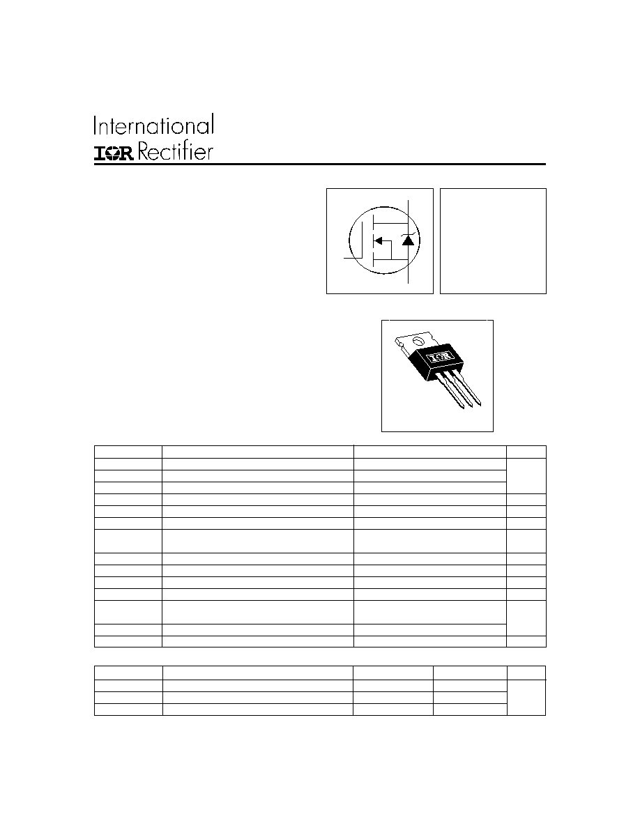
IRL3102
PRELIMINARY
HEXFET
®
Power MOSFET
PD- 9.1694A
These HEXFET Power MOSFETs were designed
specifically to meet the demands of CPU core DC-DC
converters in the PC environment. Advanced
processing techniques combined with an optimized
gate oxide design results in a die sized specifically to
offer maximum efficiency at minimum cost.
The TO-220 package is universally preferred for all
commercial-industrial applications at power
dissipation levels to approximately 50 watts. The low
thermal resistance and low package cost of the TO-
220 contribute to its wide acceptance throughout the
industry.
S
D
G
Absolute Maximum Ratings
Parameter
Typ.
Max.
Units
R
JC
Junction-to-Case
1.4
R
CS
Case-to-Sink, Flat, Greased Surface
0.50
°C/W
R
JA
Junction-to-Ambient
62
Thermal Resistance
V
DSS
= 20V
R
DS(on)
= 0.013
I
D
= 61A
TO-220AB
Description
l
Advanced Process Technology
l
Optimized for 4.5V-7.0V Gate Drive
l
Ideal for CPU Core DC-DC Converters
l
Fast Switching
IRL3102
Parameter
Min. Typ. Max. Units
Conditions
V
(BR)DSS
Drain-to-Source Breakdown Voltage
20
V
V
GS
= 0V, I
D
= 250µA
V
(BR)DSS
/
T
J
Breakdown Voltage Temp. Coefficient
0.016
V/°C
Reference to 25°C, I
D
= 1mA
0.015
V
GS
= 4.5V, I
D
= 37A
0.013
V
GS
= 7.0V, I
D
= 37A
V
GS(th)
Gate Threshold Voltage
0.70
V
V
DS
= V
GS
, I
D
= 250µA
g
fs
Forward Transconductance
36
S
V
DS
= 16V, I
D
= 35A
25
µA
V
DS
= 20V, V
GS
= 0V
250
V
DS
= 10V, V
GS
= 0V, T
J
= 150°C
Gate-to-Source Forward Leakage
100
nA
V
GS
= 10V
Gate-to-Source Reverse Leakage
-100
V
GS
= -10V
Q
g
Total Gate Charge
58
I
D
= 35A
Q
gs
Gate-to-Source Charge
14
nC
V
DS
= 16V
Q
gd
Gate-to-Drain ("Miller") Charge
21
V
GS
= 4.5V, See Fig. 6
t
d(on)
Turn-On Delay Time
10
V
DD
= 10V
t
r
Rise Time
130
ns
I
D
= 35A
t
d(off)
Turn-Off Delay Time
80
R
G
= 9.0
,
V
GS
= 4.5V
t
f
Fall Time
110
R
D
= 0.28
,
Between lead,
6mm (0.25in.)
from package
and center of die contact
C
iss
Input Capacitance
2500
V
GS
= 0V
C
oss
Output Capacitance
1000
pF
V
DS
= 15V
C
rss
Reverse Transfer Capacitance
360
= 1.0MHz, See Fig. 5
S
D
G
Repetitive rating; pulse width limited by
max. junction temperature.
I
SD
35A, di/dt
100A/µs, V
DD
V
(BR)DSS
,
T
J
150°C
Notes:
Starting T
J
= 25°C, L = 0.36mH
R
G
= 25
, I
AS
= 35A.
Pulse width
300µs; duty cycle
2%.
S
D
G
Parameter
Min. Typ. Max. Units
Conditions
I
S
Continuous Source Current
MOSFET symbol
(Body Diode)
showing the
I
SM
Pulsed Source Current
integral reverse
(Body Diode)
p-n junction diode.
V
SD
Diode Forward Voltage
1.3
V
T
J
= 25°C, I
S
= 37A, V
GS
= 0V
t
rr
Reverse Recovery Time
59
88
ns
T
J
= 25°C, I
F
= 35A
Q
rr
Reverse Recovery Charge
110
160
nC
di/dt = 100A/µs
t
on
Forward Turn-On Time
Intrinsic turn-on time is negligible (turn-on is dominated by L
S
+L
D
)
Source-Drain Ratings and Characteristics
61
240
A
Electrical Characteristics @ T
J
= 25°C (unless otherwise specified)
R
DS(on)
Static Drain-to-Source On-Resistance
I
GSS
nH
L
S
Internal Source Inductance
7.5
L
D
Internal Drain Inductance
4.5
I
DSS
Drain-to-Source Leakage Current
IRL3102
Fig 4. Normalized On-Resistance
Vs. Temperature
Fig 2. Typical Output Characteristics
Fig 1. Typical Output Characteristics
Fig 3. Typical Transfer Characteristics
10
100
1000
0.1
1
10
100
20µs PULSE WIDTH
T = 25 C
J
°
TOP
BOTTOM
VGS
15V
12V
10V
8.0V
6.0V
4.0V
3.0V
2.5V
V , Drain-to-Source Voltage (V)
I , Drain-to-Source Current (A)
DS
D
2.5V
10
100
1000
0.1
1
10
100
20µs PULSE WIDTH
T = 150 C
J
°
TOP
BOTTOM
VGS
15V
12V
10V
8.0V
6.0V
4.0V
3.0V
2.5V
V , Drain-to-Source Voltage (V)
I , Drain-to-Source Current (A)
DS
D
2.5V
1
10
100
1000
2
3
4
5
6
7
V = 15V
20µs PULSE WIDTH
DS
V , Gate-to-Source Voltage (V)
I , Drain-to-Source Current (A)
GS
D
T = 25 C
J
°
T = 150 C
J
°
-60 -40 -20
0
20
40
60
80 100 120 140 160
0.0
0.5
1.0
1.5
2.0
T , Junction Temperature( C)
R , Drain-to-Source On Resistance
(Normalized)
J
DS(on)
°
V
=
I =
GS
D
4.5V
61A
VGS
TOP 10V
8.0V
6.0V
4.0V
3.0V
BOTTOM 2.5V
VGS
TOP 10V
8.0V
6.0V
4.0V
3.0V
BOTTOM 2.5V
IRL3102
Fig 8. Maximum Safe Operating Area
Fig 6. Typical Gate Charge Vs.
Gate-to-Source Voltage
Fig 5. Typical Capacitance Vs.
Drain-to-Source Voltage
Fig 7. Typical Source-Drain Diode
Forward Voltage
1
10
100
0
600
1200
1800
2400
3000
3600
4200
V , Drain-to-Source Voltage (V)
C, Capacitance (pF)
DS
V
C
C
C
=
=
=
=
0V,
C
C
C
f = 1MHz
+ C
+ C
C SHORTED
GS
iss
gs
gd ,
ds
rss
gd
oss
ds
gd
C
iss
C
oss
C
rss
0
20
40
60
80
100
0
3
6
9
12
15
Q , Total Gate Charge (nC)
V , Gate-to-Source Voltage (V)
G
GS
I =
D
35A
V
= 16V
DS
1
10
100
1000
1
10
100
OPERATION IN THIS AREA LIMITED
BY R
DS(on)
Single Pulse
T
T
= 150 C
= 25 C
°
°
J
C
V , Drain-to-Source Voltage (V)
I , Drain Current (A)
I , Drain Current (A)
DS
D
100us
1ms
10ms
1
10
100
1000
0.2
0.8
1.4
2.0
2.6
V ,Source-to-Drain Voltage (V)
I , Reverse Drain Current (A)
SD
SD
V = 0 V
GS
T = 25 C
J
°
T = 150 C
J
°
IRL3102
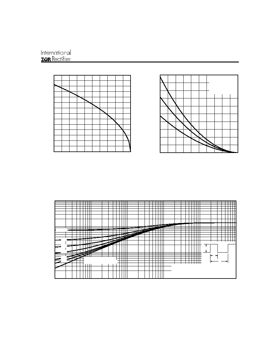
Fig 11. Maximum Effective Transient Thermal Impedance, Junction-to-Case
Fig 9. Maximum Drain Current Vs.
Case Temperature
Fig 10. Maximum Avalanche Energy
Vs. Drain Current
25
50
75
100
125
150
0
10
20
30
40
50
60
70
T , Case Temperature ( C)
I , Drain Current (A)
°
C
D
25
50
75
100
125
150
0
100
200
300
400
500
Starting T , Junction Temperature( C)
E , Single Pulse Avalanche Energy (mJ)
J
AS
°
ID
TOP
BOTTOM
16A
22A
35A
0.01
0.1
1
10
0.00001
0.0001
0.001
0.01
0.1
1
Notes:
1. Duty factor D = t / t
2. Peak T = P
x Z
+ T
1
2
J
DM
thJC
C
P
t
t
DM
1
2
t , Rectangular Pulse Duration (sec)
Thermal Response
(Z )
1
thJC
0.01
0.02
0.05
0.10
0.20
D = 0.50
SINGLE PULSE
(THERMAL RESPONSE)