
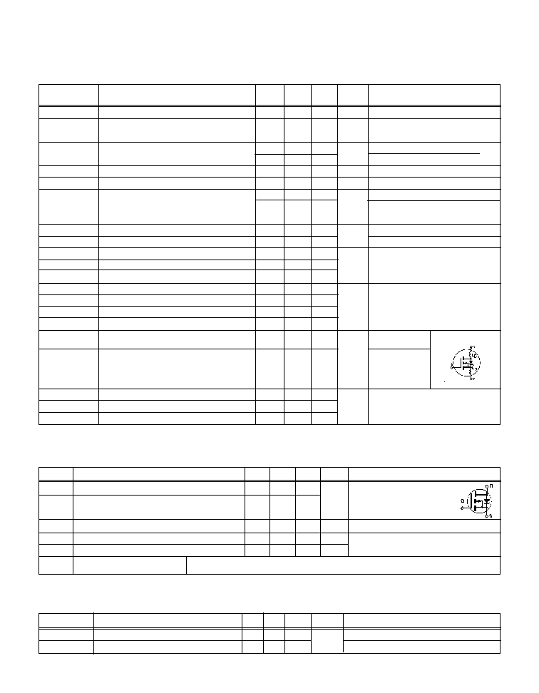
Absolute Maximum Ratings
Parameter
IRHN9150, IRHN93150
Units
ID @ VGS = -12V, TC = 25°C Continuous Drain Current
-22
ID @ VGS = -12V, TC = 100°C Continuous Drain Current
-14
IDM
Pulsed Drain Current
-88
PD @ TC = 25°C
Max. Power Dissipation
150
W
Linear Derating Factor
1.2
W/K
VGS
Gate-to-Source Voltage
±20
V
EAS
Single Pulse Avalanche Energy
500
mJ
IAR
Avalanche Current
-22
A
EAR
Repetitive Avalanche Energy
15
mJ
dv/dt
Peak Diode Recovery dv/dt
-23
V/ns
TJ
Operating Junction
-55 to 150
TSTG
Storage Temperature Range
Lead Temperature
300 (0.063 in. (1.6mm) from
case for 10 sec.)
Weight
2.6 (typical)
g
P-CHANNEL
RAD HARD
Provisional Data Sheet No. PD - 9.885B
Pre-Radiation
-100Volt, 0.075
, RAD HARD HEXFET
International Rectifier's P-Channel RAD HARD tech-
nology HEXFETs demonstrate excellent threshold
voltage stability at total radiation doses as high as 3
x 10
5
Rads (Si). Under identical pre- and post-radia-
tion test conditions, International Rectifier's P-Chan-
nel RAD HARD HEXFETs retain identical electrical
specifications up to 1 x 10
5
Rads (Si) total dose. No
compensation in gate drive circuitry is required. These
devices are also capable of surviving transient ion-
ization pulses as high as 1 x 10
12
Rads (Si)/Sec, and
return to normal operation within a few microseconds.
Since the SEE process utilizes International Rectifier's
patented HEXFET technology, the user can expect
the highest quality and reliability in the industry.
RAD HARD HEXFET transistors also feature all of
the well-established advantages of MOSFETs, such
as voltage control, very fast switching, ease of paral-
leling and temperature stability of the electrical pa-
rameters. They are well-suited for applications such
as switching power supplies, motor controls, invert-
ers, choppers, audio amplifiers and high-energy pulse
circuits in space and weapons environments.
o
C
A
REPETITIVE AVALANCHE AND dv/dt RATED
IRHN9150
HEXFET
®
TRANSISTOR
11/4/97
IRHN93150
Product Summary
Part Number
BV
DSS
R
DS(on)
I
D
IRHN9150
-100V
0.075
-22A
IRHN93150
-100V
0.075
-22A
Features:
n
Radiation Hardened up to 3 x 10
5
Rads (Si)
n
Single Event Burnout (SEB) Hardened
n
Single Event Gate Rupture (SEGR) Hardened
n
Gamma Dot (Flash X-Ray) Hardened
n
Neutron Tolerant
n
Identical Pre- and Post-Electrical Test Conditions
n
Repetitive Avalanche Rating
n
Dynamic dv/dt Rating
n
Simple Drive Requirements
n
Ease of Paralleling
n
Hermetically Sealed
n
Surface Mount
n
Lightweight
IRHN9150, IRHN93150 Device
Pre-Radiation
Electrical Characteristics
@ Tj = 25°C (Unless Otherwise Specified)
Parameter
Min
Typ Max Units
Test Conditions
BVDSS
Drain-to-Source Breakdown Voltage
-100
--
--
V
VGS = 0V, ID = -1.0mA
BVDSS/
TJ Temperature Coefficient of Breakdown
--
-0.093
--
V/°C
Reference to 25°C, ID = -1.0mA
Voltage
RDS(on)
Static Drain-to-Source
--
--
0.075
VGS = -12V, ID = -14A
On-State Resistance
--
--
0.080
VGS = -12V, ID = -22A
VGS(th)
Gate Threshold Voltage
-2.0
--
-4.0
V
VDS = VGS, ID = -1.0mA
gfs
Forward Transconductance
11
--
--
S (
)
VDS > -15V, IDS = -14A
IDSS
Zero Gate Voltage Drain Current
--
--
-25
VDS= 0.8 x Max Rating,VGS=0V
--
--
-250
VDS = 0.8 x Max Rating
VGS = 0V, TJ = 125°C
IGSS
Gate-to-Source Leakage Forward
--
--
-100
VGS = -20V
IGSS
Gate-to-Source Leakage Reverse
--
--
100
VGS = 20V
Qg
Total Gate Charge
--
--
200
VGS =-12V, ID = -22A
Qgs
Gate-to-Source Charge
--
--
35
nC
VDS = Max Rating x 0.5
Qgd
Gate-to-Drain (`Miller') Charge
--
--
48
td
(on)
Turn-On Delay Time
--
--
40
VDD = -50V, ID =-22A,
tr
Rise Time
--
--
150
RG = 2.35
td
(off)
Turn-Off Delay Time
--
--
100
tf
Fall Time
--
--
190
LD
Internal Drain Inductance
--
0.8
--
LS
Internal Source Inductance
--
2.8
--
Ciss
Input Capacitance
--
4300
--
VGS = 0V, VDS = -25V
Coss
Output Capacitance
--
1100
--
pF
f = 1.0MHz
Crss
Reverse Transfer Capacitance
--
310
--
nA
nH
ns
Measured from center of drain
pad to die.
Measured from center of
source pad to the end of
source bonding wire
Modified MOSFET symbol show-
ing the internal inductances.
µ
A
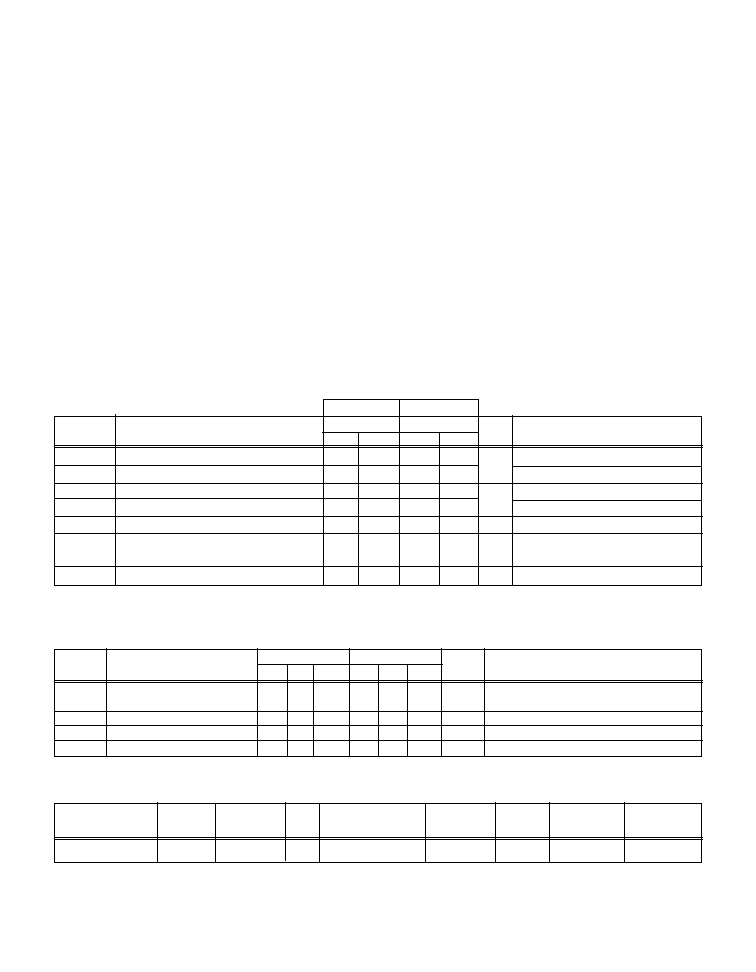
Source-Drain Diode Ratings and Characteristics
Parameter
Min Typ
Max Units
Test Conditions
IS
Continuous Source Current (Body Diode)
--
--
-22
Modified MOSFET symbol showing the integra
l
ISM
Pulse Source Current (Body Diode)
--
--
-88
r
everse p-n junction rectifier.
VSD
Diode Forward Voltage
--
--
-3.0
V
T
j
= 25°C, IS = -22A, VGS = 0V
trr
Reverse Recovery Time
--
--
250
ns
Tj = 25°C, IF = -22A, di/dt
-100A/
µ
s
QRR
Reverse Recovery Charge
--
--
1.5
µ
C
VDD
-50V
ton
Forward Turn-On Time
Intrinsic turn-on time is negligible. Turn-on speed is substantially controlled by LS + LD.
A
Thermal Resistance
Parameter
Min Typ Max
Units
Test Conditions
RthJC
Junction-to-Case
--
--
0.83
RthJ-PCB
Junction-to-PC board
--
6.6
-- Soldered to a 1 inch square clad PC board
K/W
IRHN9150, IRHN93150 Device
Table 2. High Dose Rate
10
11
Rads (Si)/sec 10
12
Rads (Si)/sec
Parameter
Min Typ Max
Min Typ Max
Units
Test Conditions
V
DSS
Drain-to-Source Voltage
--
--
-80
--
--
-80
V
Applied drain-to-source voltage during
gamma-dot
IPP
--
-100
--
--
-100
--
A
Peak radiation induced photo-current
di/dt
--
--
-800
--
--
-160 A/µsec Rate of rise of photo-current
L1
0.1
--
--
0.5
--
--
µH
Circuit inductance required to limit di/dt
Table 3. Single Event Effects
LET (Si)
Fluence
Range
V
DS
Bias
V
GS
Bias
Parameter
Typical
Units
Ion
(MeV/mg/cm
2
)
(ions/cm
2
)
(µm)
(V)
(V)
BV
DSS
-100
V
Ni
28
1 x 10
5
~41
-100
+5
Radiation Performance of P-Channel Rad
Hard HEXFETs
International Rectifier Radiation Hardened HEXFETs
are tested to verify their hardness capability. The hard-
ness assurance program at International Rectifier uses
two radiation environments.
Every manufacturing lot is tested in a low dose rate
(total dose) environment per MlL-STD-750, test
method 1019. International Rectifier has imposed a
standard gate voltage of 12 volts per note 6 and a
V
DSS
bias condition equal to 80% of the device rated
voltage per note 7. Pre- and post-radiation limits of
the devices irradiated to 1 x 10
5
Rads (Si) are identi-
cal and are presented in Table 1, column 1, IRHN9150.
The values in Table 1 will be met for either of the two
low dose rate test circuits that are used. Both pre-
and post-radiation performance are tested and speci-
fied using the same drive circuitry and test conditions
in order to provide a direct comparison. It should be
noted that at a radiation level of 3 x 10
5
Rads (Si) no
changes in limits are specified in DC parameters.
High dose rate testing may be done on a special
request basis using a dose rate up to 1 x 10
12
Rads
(Si)/Sec.
International Rectifier radiation hardened P-Channel
HEXFETS are considered to be neutron -tolerant, as
stated in MIL-PRF-19500 Group D. International Rec-
tifier radiation hardened P-Channel HEXFETs have
been characterized in heavy ion Single Event Effects
(SEE) environments and the results are shown in
Table 3.
Table 1. Low Dose Rate
IRHN9150 IRHN93150
Parameter
100K Rads (Si) 300K Rads (Si)
Units
Test Conditions
Min
Max
Min
Max
BV
DSS
Drain-to-Source Breakdown Voltage
-100
--
-100
--
V
V
GS
= 0V, I
D
= -1.0mA
V
GS(th)
Gate Threshold Voltage
-2.0
-4.0
-2.0
-5.0
V
GS
= V
DS
, I
D
= -1.0mA
I
GSS
Gate-to-Source Leakage Forward
--
-100
--
-100
nA
V
GS
= -20V
I
GSS
Gate-to-Source Leakage Reverse
--
100
--
100
V
GS
= 20 V
I
DSS
Zero Gate Voltage Drain Current
--
-25
--
-25
µA
V
DS
=0.8 x Max Rating, V
GS
=0V
R
DS(on)1
Static Drain-to-Source
--
0.075
--
0.085
V
GS
= -12V, I
D
= -14A
On-State Resistance One
V
SD
Diode Forward Voltage
--
-3.0
--
-3.0
V
TC = 25°C, IS = -22A,V
GS
= 0V
Radiation Characteristics

IRHN9150, IRHN93150 Device
Pre-Radiation
10
100
5
6
7
8
9
10
V = -50V
20µs PULSE WIDTH
DS
V , Gate-to-Source Voltage (V)
I , Drain-to-Source Current (A)
GS
D
T = 25 C
J
°
T = 150 C
J
°
Fig 4. Normalized On-Resistance
Vs. Temperature
Fig 2. Typical Output Characteristics
Fig 1. Typical Output Characteristics
Fig 3. Typical Transfer Characteristics
10
100
1
10
100
20µs PULSE WIDTH
T = 25 C
J
°
TOP
BOTTOM
VGS
-15V
-12V
-10V
-9.0V
-8.0V
-7.0V
-6.0V
-5.0V
-V , Drain-to-Source Voltage (V)
-I , Drain-to-Source Current (A)
DS
D
-5.0V
10
100
1
10
100
20µs PULSE WIDTH
T = 150 C
J
°
TOP
BOTTOM
VGS
-15V
-12V
-10V
-9.0V
-8.0V
-7.0V
-6.0V
-5.0V
-V , Drain-to-Source Voltage (V)
-I , Drain-to-Source Current (A)
DS
D
-5.0V
-60 -40 -20
0
20
40
60
80 100 120 140 160
0.0
0.5
1.0
1.5
2.0
2.5
3.0
T , Junction Temperature( C)
R , Drain-to-Source On Resistance
(Normalized)
J
DS(on)
°
V
=
I =
GS
D
-12V
-22A
-
-

IRHN9150, IRHN93150 Device
Fig 8. Maximum Safe Operating Area
Fig 6. Typical Gate Charge Vs.
Gate-to-Source Voltage
Fig 5. Typical Capacitance Vs.
Drain-to-Source Voltage
Fig 7. Typical Source-Drain Diode
Forward Voltage
1
10
100
0
1000
2000
3000
4000
5000
6000
7000
-V , Drain-to-Source Voltage (V)
C, Capacitance (pF)
DS
V
C
C
C
=
=
=
=
0V,
C
C
C
f = 1MHz
+ C
+ C
C SHORTED
GS
iss
gs
gd ,
ds
rss
gd
oss
ds
gd
C
iss
C
oss
C
rss
0
40
80
120
160
200
0
4
8
12
16
20
Q , Total Gate Charge (nC)
-V , Gate-to-Source Voltage (V)
G
GS
FOR TEST CIRCUIT
SEE FIGURE
I =
D
13
-22A
V
=-20V
DS
V
=-50V
DS
V
=-80V
DS
1
10
100
0.0
1.0
2.0
3.0
4.0
-V ,Source-to-Drain Voltage (V)
-I , Reverse Drain Current (A)
SD
SD
V = 0 V
GS
T = 25 C
J
°
T = 150 C
J
°
1
10
100
1000
1
10
100
1000
OPERATION IN THIS AREA LIMITED
BY R
DS(on)
Single Pulse
T
T
= 150 C
= 25 C
°
°
J
C
-V , Drain-to-Source Voltage (V)
-I , Drain Current (A)
I , Drain Current (A)
DS
D
100us
1ms
10ms
Pre-Radiation