Product Summary
Part Number
BV
DSS
R
DS(on)
I
D
IRHN9230
-200V
0.8
-6.5A
Features:
n
Radiation Hardened up to 1 x 10
5
Rads (Si)
n
Single Event Burnout (SEB) Hardened
n
Single Event Gate Rupture (SEGR) Hardened
n
Gamma Dot (Flash X-Ray) Hardened
n
Neutron Tolerant
n
Identical Pre- and Post-Electrical Test Conditions
n
Repetitive Avalanche Rating
n
Dynamic dv/dt Rating
n
Simple Drive Requirements
n
Ease of Paralleling
n
Hermetically Sealed
n
Surface Mount
n
Light-weight
REPETITIVE AVALANCHE AND dv/dt RATED
HEXFET
®
TRANSISTOR
Provisional Data Sheet No. PD-9.1445
P-CHANNEL
RAD HARD
-200 Volt, 0.8
,
RAD HARD HEXFET
International Rectifier's P-Channel RAD HARD technology
HEXFETs demonstrate excellent threshold voltage stability
and breakdown voltage stability at total radiation doses as
high as 10
5
Rads (Si). Under identical pre- and post-radiation
test conditions, International Rectifier's P-Channel RAD
HARD HEXFETs retain identical electrical specifications up
to 1 x 10
5
Rads (Si) total dose. No compensation in gate
drive circuitry is required. In addition these devices are also
capable of surviving transient ionization pulses as high as
1 x 10
12
Rads (Si)/Sec, and return to normal operation within
a few microseconds. Single Event Effect (SEE) testing of
International Rectifier P-Channel RAD HARD HEXFETs has
demonstrated virtual immunity to SEE failure. Since the
P-Channel RAD HARD process utilizes International
Rectifier's patented HEXFET technology, the user can expect
the highest quality and reliability in the industry.
P-Channel RAD HARD HEXFET transistors also feature all
of the well-established advantages of MOSFETs, such as
voltage control,very fast switching, ease of paralleling and
temperature stability of the electrical parameters.
They are well-suited for applications such as switching
power supplies, motor controls, inverters, choppers, audio
amplifiers and high-energy pulse circuits in space and
weapons environments.
IRHN9230
Pre-Radiation
Notes: See page 4
o
C
A
Absolute Maximum Ratings
Parameter
IRHN9230
Units
ID @ VGS = -12V, TC = 25°C Continuous Drain Current
-6.5
ID @ VGS = -12V, TC = 100°C Continuous Drain Current
-4.0
IDM
Pulsed Drain Current
-26
PD @ TC = 25°C
Max. Power Dissipation
75
W
Linear Derating Factor
0.6
W/K
VGS
Gate-to-Source Voltage
±20
V
EAS
Single Pulse Avalanche Energy
150
mJ
IAR
Avalanche Current
-6.5
A
EAR
Repetitive Avalanche Energy
7.5
mJ
dv/dt
Peak Diode Recovery dv/dt
-5.0
V/ns
TJ
Operating Junction
-55 to 150
TSTG
Storage Temperature Range
Package Mounting
300 (for 5 seconds)
Surface Temperature
Weight
2.6 (typical)
g
Next Data Sheet
Index
Previous Datasheet
To Order
Electrical Characteristics
@ Tj = 25°C (Unless Otherwise Specified)
Parameter
Min.
Typ. Max. Units
Test Conditions
BVDSS
Drain-to-Source Breakdown Voltage
-200
--
--
V
VGS = 0V, ID = -1.0 mA
BVDSS/
TJ Temperature Coefficient of Breakdown
--
-0.22
--
V/°C
Reference to 25°C, ID = -1.0 mA
Voltage
RDS(on)
Static Drain-to-Source
--
--
0.8
VGS = -12V, ID = -4.0A
On-State Resistance
--
--
0.92
VGS = -12V, ID = -6.5A
VGS(th)
Gate Threshold Voltage
-2.0
--
-4.0
V
VDS = VGS, ID = -1.0 mA
gfs
Forward Transconductance
2.5
--
--
S (
)
VDS > -15V, IDS = -4.0 A
IDSS
Zero Gate Voltage Drain Current
--
--
-25
VDS = 0.8 x Max. Rating,VGS = 0V
--
--
-250
VDS = 0.8 x Max. Rating
VGS = 0V, TJ = 125°C
IGSS
Gate-to-Source Leakage Forward
--
--
-100
VGS = -20V
IGSS
Gate-to-Source Leakage Reverse
--
--
100
VGS = 20V
Qg
Total Gate Charge
--
--
45
VGS = -12V, ID = -6.5A
Qgs
Gate-to-Source Charge
--
--
10
VDS = Max. Rating x 0.5
Qgd
Gate-to-Drain ("Miller") Charge
--
--
25
td(on)
Turn-On Delay Time
--
--
50
VDD = 100V, ID = -6.5A, RG = 7.5
tr
Rise Time
--
--
90
td(off)
Turn-Off Delay Time
--
--
90
tf
Fall Time
--
--
90
LD
Internal Drain Inductance
--
TBD
--
LS
Internal Source Inductance
--
TBD
--
Ciss
Input Capacitance
--
1100
--
VGS = 0V, VDS = -25V
Coss
Output Capacitance
--
310
--
f = 1.0 MHz
Crss
Reverse Transfer Capacitance
--
55
--
Source-Drain Diode Ratings and Characteristics
Parameter
Min. Typ. Max. Units
Test Conditions
IS
Continuous Source Current
--
--
-6.5
Modified MOSFET symbol
(Body Diode)
showing the integral Reverse
ISM
Pulse Source Current
--
--
-26
p-n junction rectifier.
(Body Diode)
VSD
Diode Forward Voltage
--
--
-5.0
V
T
j
= 25°C, IS = -6.5A, VGS = 0V
trr
Reverse Recovery Time
--
--
400
ns
Tj = 25°C, IF = -6.5A, di/dt
-100 A/
µ
s
QRR
Reverse Recovery Charge
--
--
3.0
µ
C
VDD
-50V
ton
Forward Turn-On Time
Intrinsic turn-on time is negligible. Turn-on speed is substantially controlled by LS + LD.
Thermal Resistance
RthJC
Junction-to-Case
--
--
1.67
RthJ-PCB
Junction-to-PC board
--
TBD
--
Soldered to a copper-clad PC board
IRHN9230 Device
Pre-Radiation
µ
A
nC
pF
nH
ns
Measured from the
drain lead, 6mm (0.25
in.) from package to
center of die.
Measured from the
source lead, 6mm
(0.25 in.) from package
to source bonding pad.
Modified MOSFET
symbol showing the
internal inductances.
nA
Parameter
Min. Typ. Max. Units
Test Conditions
Notes: See page 4
A
K/W
Next Data Sheet
Index
Previous Datasheet
To Order
International Rectifier Radiation Hardened HEXFETs
are tested to verify their hardness capability. The
hardness assurance program at International Rectifier
uses two radiation environments.
Every manufacturing lot is tested in a low dose rate
(total dose) environment per MlL-STD-750, test method
1019. International Rectifier has imposed a standard
gate voltage of -12 volts per note 6 and a VDSS bias
condition equal to 80% of the device rated voltage per
note 7. Pre- and post-radiation limits of the devices
irradiated to 1 x 10
5
Rads (Si) are identical and are
presented in Table 1. The values in Table 1 will be met
for either of the two low dose rate test circuits that are
used.
Radiation Performance of P-Channel Rad
Hard HEXFETs
Both pre- and post-radiation performance are tested
and specified using the same drive circuitry and test
conditions in order to provide a direct comparison. It
should be noted that at a radiation level of 1 x 10
5
Rads (Si), no change in limits are specified in DC
parameters.
High dose rate testing may be done on a special
request basis, using a dose rate up to 1 x 10
12
Rads
(Si)/Sec.
International Rectifier radiation hardened P-Channel
HEXFETs are considered to be neutron-tolerant, as
stated in MIL-PRF-19500 Group D. International
Rectifier P-Channel radiation hardened HEXFETs
have been characterized in heavy ion Single Event
Effects environment the results are shown in Table 3.
IRHN9230 Device
Radiation Characteristics
V
nA
Table 1. Low Dose Rate
IRHN9230
Parameter
100K Rads (Si)
Units
Test Conditions
min.
max.
BV
DSS
Drain-to-Source Breakdown Voltage
-200
--
V
GS
= 0V, I
D
= -1.0 mA
V
GS(th)
Gate Threshold Voltage
-2.0
-4.0
V
GS
= V
DS
, I
D
= -1.0 mA
I
GSS
Gate-to-Source Leakage Forward
--
-100
V
GS
= -20V
I
GSS
Gate-to-Source Leakage Reverse
--
100
V
GS
= 20V
I
DSS
Zero Gate Voltage Drain Current
--
-25
µA
V
DS
= 0.8 x Max Rating, V
GS
= 0V
R
DS(on)1
Static Drain-to-Source
--
0.8
V
GS
= -12V, I
D
= -4.0A
On-State Resistance One
V
SD
Diode Forward Voltage
--
-5.0
V
T
C
= 25°C, I
S
= -6.5A,V
GS
= 0V
Table 2. High Dose Rate
10
11
Rads (Si)/sec10
12
Rads (Si)/sec
Parameter
Min. Typ Max. Min.Typ. Max. Units
Test Conditions
VDSS
Drain-to-Source Voltage
--
--
-160
--
--
-160
V
Applied drain-to-source voltage
during gamma-dot
IPP
--
-60
--
--
-60
--
A
Peak radiation induced photo-current
di/dt
--
-800
--
--
-160
--
A/µsec Rate of rise of photo-current
L1
27
--
--
0.5
--
--
µH
Circuit inductance required to limit di/dt
Table 3. Single Event Effects
LET (Si)
Fluence
Range
V
DS
Bias
V
GS
Bias
Parameter
Typ.
Units
Ion
(MeV/mg/cm
2
)
(ions/cm
2
)
(
µ
m)
(V)
(V)
BVDSS
-200
V
Ni
28
1 x 10
5
~41
-200
+5
To Order
Next Data Sheet
Index
Previous Datasheet
IRHN9230 Device
Radiation Characteristics
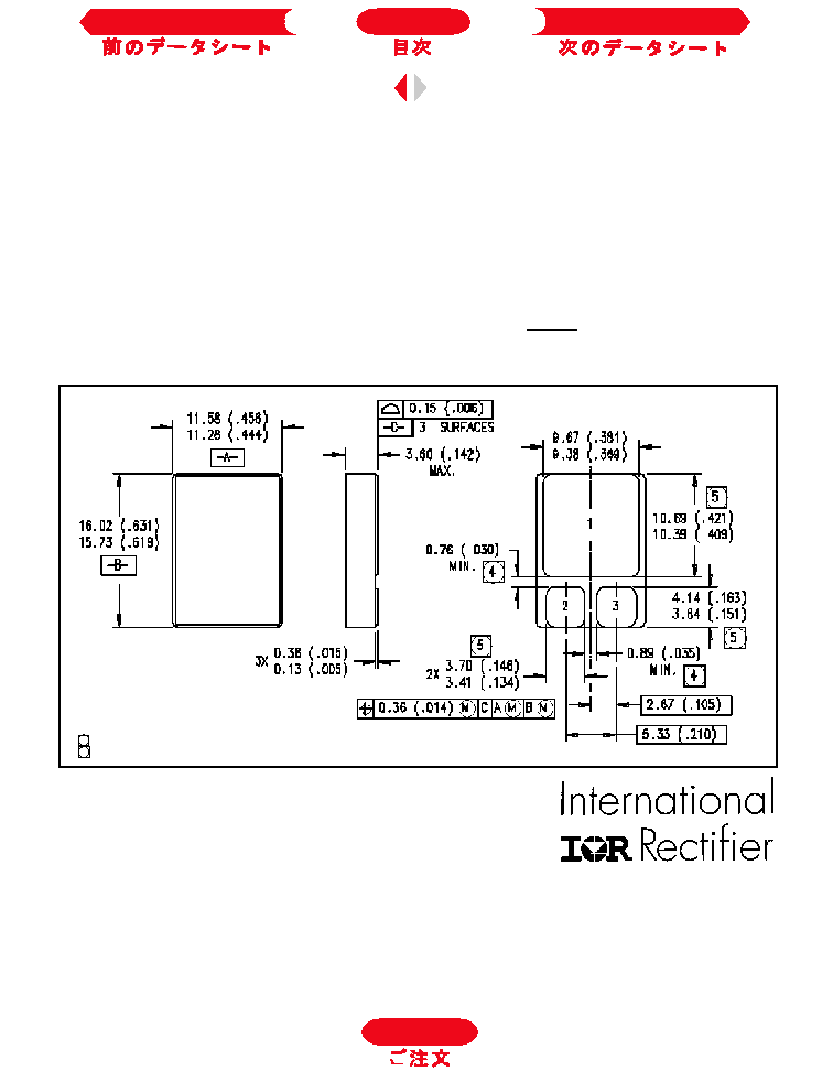
Case Outline and Dimensions -- SMD-1
Repetitive Rating; Pulse width limited by
maximum junction temperature.
Refer to current HEXFET reliability report.
@ VDD = -50V, Starting TJ = 25°C,
EAS = [0.5 * L * (I
L
2
) * [BVDSS/(BVDSS-VDD)]
25
RG
200
, IL = -6.5A, VGS = -12V
ISD
-6.5A, di/dt
-140 A/
µ
s,
VDD
BVDSS, TJ
150°C
Pulse width
300
µ
s; Duty Cycle
2%
K/W = °C/W
W/K = W/°C
Total Dose Irradiation with VGS Bias.
-12 volt VGS applied and VDS = 0 during
irradiation per MIL-STD-750, method 1019.
Total Dose Irradiation with VDS Bias.
VDS = 0.8 rated BVDSS (pre-radiation)
applied and VGS = 0 during irradiation per
MlL-STD-750, method 1019.
This test is performed using a flash x-ray
source operated in the e-beam mode (energy
~2.5 MeV), 30 nsec pulse.
Process characterized by independent laboratory.
All Pre-Radiation and Post-Radiation test
conditions are identical to facilitate direct
comparison for circuit applications.
WORLD HEADQUARTERS: 233 Kansas St., El Segundo, California 90245, Tel: (310) 322 3331
EUROPEAN HEADQUARTERS: Hurst Green, Oxted, Surrey RH8 9BB, UK Tel: ++ 44 1883 713215
IR CANADA: 7321 Victoria Park Ave., Suite 201, Markham, Ontario L3R 2Z8, Tel: (905) 475 1897
IR GERMANY: Saalburgstrasse 157, 61350 Bad Homburg Tel: ++ 49 6172 96590
IR ITALY: Via Liguria 49, 10071 Borgaro, Torino Tel: ++ 39 11 451 0111
IR FAR EAST: K&H Bldg., 2F, 3-30-4 Nishi-Ikeburo 3-Chome, Toshima-Ku, Tokyo, Japan 171 Tel: ++ 81 3 3983 0641
IR SOUTHEAST ASIA: 315 Outram Road, #10-02 Tan Boon Liat Building, Singapore 0316 Tel: ++ 65 221 8371
http://www/irf.com/
Data and specifications subject to change without notice. 6/96
Notes:
1. Dimensioning and Tolerancing per ANSI Y14.5M-1982
2. Controlling Dimension: Inch
3. Dimensions are shown in millimeters (Inches)
4 Dimension includes metallization flash
5 Dimension does not include metallization flash
To Order
Next Data Sheet
Index
Previous Datasheet