Äîêóìåíòàöèÿ è îïèñàíèÿ www.docs.chipfind.ru
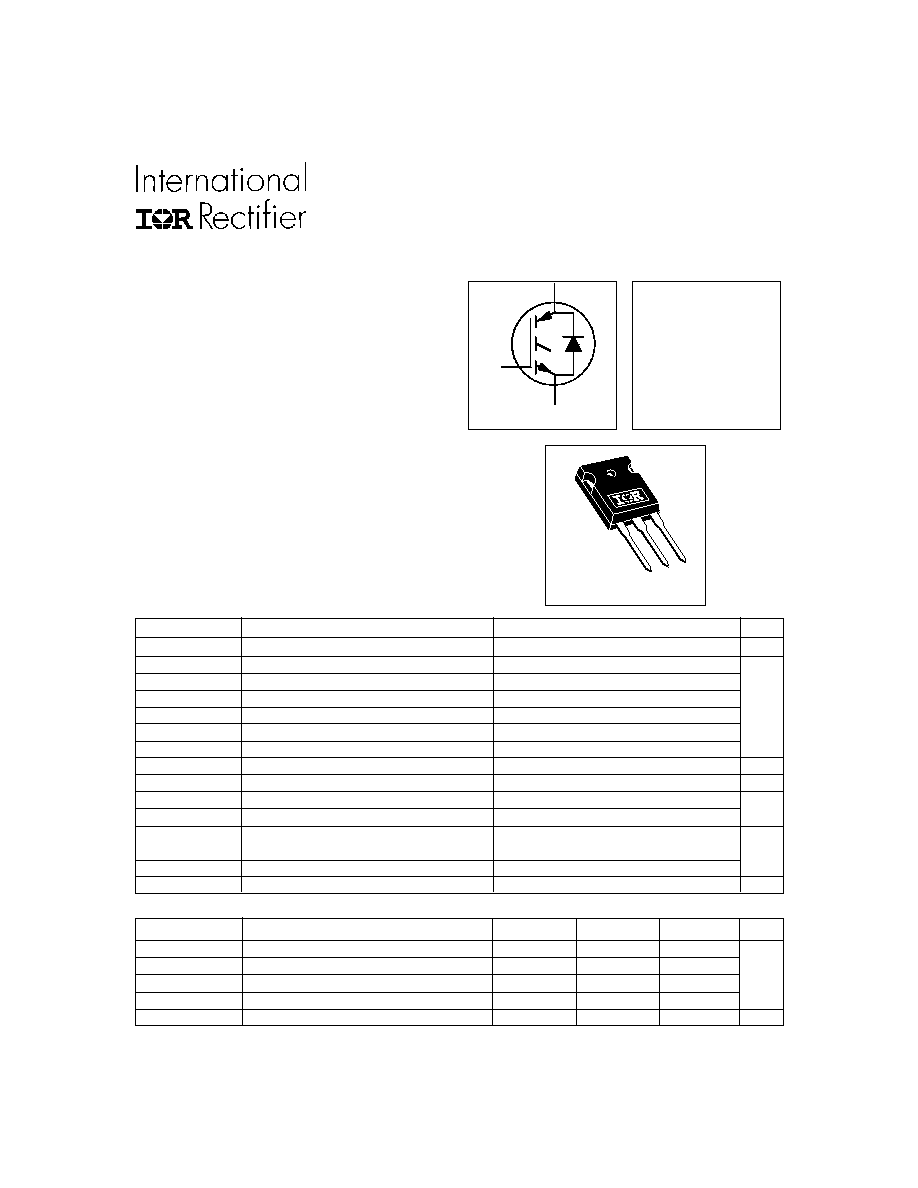
IRG4PH50KD
INSULATED GATE BIPOLAR TRANSISTOR WITH
ULTRAFAST SOFT RECOVERY DIODE
E
G
n-ch an nel
C
V
CES
= 1200V
V
CE(on) typ.
= 2.77V
@V
GE
= 15V, I
C
= 24A
PD- 91575B
TO-247AC
Short Circuit Rated
UltraFast IGBT
Parameter
Max.
Units
V
CES
Collector-to-Emitter Voltage
1200
V
I
C
@ T
C
= 25°C
Continuous Collector Current
45
I
C
@ T
C
= 100°C
Continuous Collector Current
24
I
CM
Pulsed Collector Current
Q
90
A
I
LM
Clamped Inductive Load Current
R
90
I
F
@ T
C
= 100°C
Diode Continuous Forward Current
16
I
FM
Diode Maximum Forward Current
90
t
sc
Short Circuit Withstand Time
10
µs
V
GE
Gate-to-Emitter Voltage
± 20
V
P
D
@ T
C
= 25°C
Maximum Power Dissipation
200
P
D
@ T
C
= 100°C
Maximum Power Dissipation
78
T
J
Operating Junction and
-55 to +150
T
STG
Storage Temperature Range
°C
Soldering Temperature, for 10 sec.
300 (0.063 in. (1.6mm) from case)
Mounting Torque, 6-32 or M3 Screw.
10 lbf·in (1.1 N·m)
7/7/2000
Parameter
Min.
Typ.
Max.
Units
R
JC
Junction-to-Case - IGBT
0.64
R
JC
Junction-to-Case - Diode
0.83
°C/W
R
CS
Case-to-Sink, flat, greased surface
0.24
R
JA
Junction-to-Ambient, typical socket mount
40
Wt
Weight
6 (0.21)
g (oz)
Thermal Resistance
Absolute Maximum Ratings
W
Features
Features
Features
Features
Features
· High short circuit rating optimized for motor control,
t
sc
=10µs, V
CC
= 720V , T
J
= 125°C,
V
GE
= 15V
· Combines low conduction losses with high
switching speed
· Tighter parameter distribution and higher efficiency
than previous generations
· IGBT co-packaged with HEXFRED
TM
ultrafast,
ultrasoft recovery antiparallel diodes
· Latest generation 4 IGBT's offer highest power density
motor controls possible
· HEXFRED
TM
diodes optimized for performance with IGBTs.
Minimized recovery characteristics reduce noise, EMI and
switching losses
· This part replaces the IRGPH50KD2 and IRGPH50MD2
products
· For hints see design tip 97003
Benefits
www.irf.com
1
IRG4PH50KD
2
www.irf.com
Parameter
Min. Typ. Max. Units
Conditions
Q
g
Total Gate Charge (turn-on)
--
180
270
I
C
= 24A
Q
ge
Gate - Emitter Charge (turn-on)
--
25
38
nC
V
CC
= 400V
See Fig.8
Q
gc
Gate - Collector Charge (turn-on)
--
70
110
V
GE
= 15V
t
d(on)
Turn-On Delay Time
--
87
--
t
r
Rise Time
--
100
--
T
J
= 25°C
t
d(off)
Turn-Off Delay Time
--
140
300
I
C
= 24A, V
CC
= 800V
t
f
Fall Time
--
200
300
V
GE
= 15V, R
G
= 5.0
E
on
Turn-On Switching Loss
--
3.83
--
Energy losses include "tail"
E
off
Turn-Off Switching Loss
--
1.90
--
mJ
and diode reverse recovery
E
ts
Total Switching Loss
--
5.73
7.9
See Fig. 9,10,18
t
sc
Short Circuit Withstand Time
10
--
--
µs
V
CC
= 720V, T
J
= 125°C
V
GE
= 15V, R
G
= 5.0
t
d(on)
Turn-On Delay Time
--
67
--
T
J
= 150°C, See Fig. 10,11,18
t
r
Rise Time
--
72
--
I
C
= 24A, V
CC
= 800V
t
d(off)
Turn-Off Delay Time
--
310
--
V
GE
= 15V, R
G
= 5.0
,
t
f
Fall Time
--
390
--
Energy losses include "tail"
E
ts
Total Switching Loss
--
8.36
--
mJ
and diode reverse recovery
L
E
Internal Emitter Inductance
--
13
--
nH
Measured 5mm from package
C
ies
Input Capacitance
--
2800
--
V
GE
= 0V
C
oes
Output Capacitance
--
140
--
pF
V
CC
= 30V
See Fig. 7
C
res
Reverse Transfer Capacitance
--
53
--
= 1.0MHz
t
rr
Diode Reverse Recovery Time
--
90
135
ns
T
J
= 25°C See Fig.
--
164
245
T
J
= 125°C 14 I
F
= 16A
I
rr
Diode Peak Reverse Recovery Current
--
5.8
10
A
T
J
= 25°C See Fig.
--
8.3
15
T
J
= 125°C 15 V
R
= 200V
Q
rr
Diode Reverse Recovery Charge
--
260
675
nC
T
J
= 25°C See Fig.
--
680 1838
T
J
= 125°C 16 di/dt = 200A/µs
di
(rec)M
/dt
Diode Peak Rate of Fall of Recovery
--
120
--
A/µs
T
J
= 25°C See Fig.
During t
b
--
76
--
T
J
= 125°C 17
Switching Characteristics @ T
J
= 25°C (unless otherwise specified)
ns
ns
Parameter
Min. Typ. Max. Units
Conditions
V
(BR)CES
Collector-to-Emitter Breakdown Voltage
S 1200 --
--
V
V
GE
= 0V, I
C
= 250µA
V
(BR)CES
/
T
J
Temperature Coeff. of Breakdown Voltage
--
0.91
--
V/°C
V
GE
= 0V, I
C
= 1.0mA
V
CE(on)
Collector-to-Emitter Saturation Voltage
--
2.77
3.5
I
C
= 24A
V
GE
= 15V
--
3.28
--
V
I
C
= 45A
See Fig. 2, 5
--
2.54
--
I
C
= 24A, T
J
= 150°C
V
GE(th)
Gate Threshold Voltage
3.0
--
6.0
V
CE
= V
GE
, I
C
= 250µA
V
GE(th)
/
T
J
Temperature Coeff. of Threshold Voltage
--
-10
--
mV/°C V
CE
= V
GE
, I
C
= 250µA
g
fe
Forward Transconductance
T
13
19
--
S
V
CE
= 100V, I
C
= 24A
I
CES
Zero Gate Voltage Collector Current
--
--
250
µA
V
GE
= 0V, V
CE
= 1200V
--
--
6500
V
GE
= 0V, V
CE
= 1200V, T
J
= 150°C
V
FM
Diode Forward Voltage Drop
--
2.5
3.5
V
I
C
= 16A
See Fig. 13
--
2.1
3.0
I
C
= 16A, T
J
= 150°C
I
GES
Gate-to-Emitter Leakage Current
--
--
±100
nA
V
GE
= ±20V
Electrical Characteristics @ T
J
= 25°C (unless otherwise specified)
IRG4PH50KD
www.irf.com
3
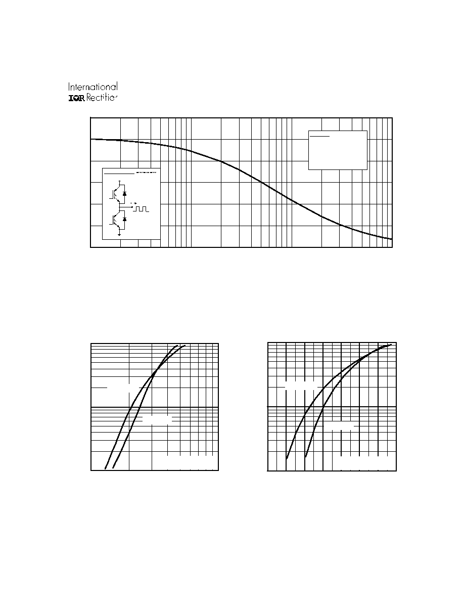
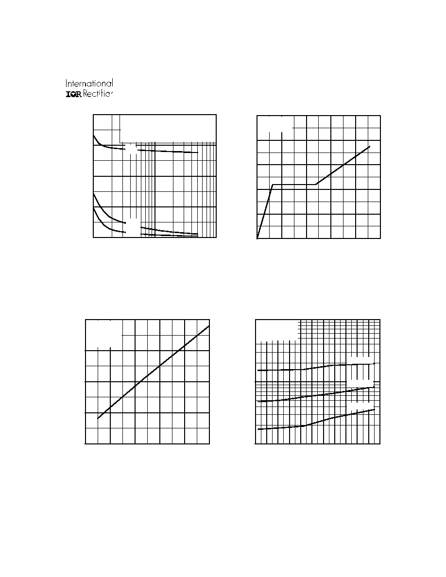
Fig. 1 - Typical Load Current vs. Frequency
(Load Current = I
RMS
of fundamental)
Fig. 2 - Typical Output Characteristics
Fig. 3 - Typical Transfer Characteristics
1
10
100
1
10
V , Collector-to-Emitter Voltage (V)
I , Collector-to-Emitter Current (A)
CE
C
V = 15V
20µs PULSE WIDTH
GE
T = 25 C
J
°
T = 150 C
J
°
1
10
100
5
6
7
8
9
10
11
12
V , Gate-to-Emitter Voltage (V)
I , Collector-to-Emitter Current (A)
GE
C
V = 50V
5µs PULSE WIDTH
CC
T = 25 C
J
°
T = 150 C
J
°
0.1
1
10
100
0
5
10
15
20
25
30
f, Frequency (KHz)
LOAD CURRENT (A)
F o r b o th :
D u ty c y c le : 5 0 %
T = 1 2 5 ° C
T = 9 0 ° C
G a te d riv e a s s p e c ifie d
sink
J
P o w e r D is s ip a tio n = W
6 0% of rate d
volta ge
I
Id e a l d io d e s
S q u a re w a v e :
40
IRG4PH50KD
4
www.irf.com
Fig. 6 - Maximum Effective Transient Thermal Impedance, Junction-to-Case
Fig. 5 - Typical Collector-to-Emitter Voltage
vs. Junction Temperature
Fig. 4 - Maximum Collector Current vs. Case
Temperature
25
50
75
100
125
150
0
10
20
30
40
50
T , Case Temperature ( C)
Maximum DC Collector Current(A)
C
°
0.001
0.01
0.1
1
0.00001
0.0001
0.001
0.01
0.1
1
Notes:
1. Duty factor D = t / t
2. Peak T = P
x Z
+ T
1
2
J
DM
thJC
C
P
t
t
DM
1
2
t , Rectangular Pulse Duration (sec)
Thermal Response (Z )
1
thJC
0.01
0.02
0.05
0.10
0.20
D = 0.50
SINGLE PULSE
(THERMAL RESPONSE)
-60 -40 -20
0
20
40
60
80 100 120 140 160
1.5
2.0
2.5
3.0
3.5
4.0
T , Junction Temperature ( C)
V , Collector-to-Emitter Voltage(V)
J
°
CE
V = 15V
80 us PULSE WIDTH
GE
I = A
48
C
I = A
24
C
I = A
12
C
IRG4PH50KD
www.irf.com
5
-60 -40 -20
0
20
40
60
80 100 120 140 160
1
10
100
T , Junction Temperature ( C )
Total Switching Losses (mJ)
J
°
R = Ohm
V = 15V
V = 960V
G
GE
CC
I = A
48
C
I = A
24
C
I = A
12
C
0
10
20
30
40
50
5.4
5.8
6.2
6.6
7.0
R , Gate Resistance (Ohm)
Total Switching Losses (mJ)
G
V = 960V
V = 15V
T = 25 C
I = 24A
CC
GE
J
C
°
Fig. 7 - Typical Capacitance vs.
Collector-to-Emitter Voltage
Fig. 8 - Typical Gate Charge vs.
Gate-to-Emitter Voltage
Fig. 9 - Typical Switching Losses vs. Gate
Resistance
Fig. 10 - Typical Switching Losses vs.
Junction Temperature
0
40
80
120
160
200
0
4
8
12
16
20
Q , Total Gate Charge (nC)
V , Gate-to-Emitter Voltage (V)
G
GE
V
= 400V
I
= 24A
CC
C
5.0
1
10
100
0
1000
2000
3000
4000
V , Collector-to-Emitter Voltage (V)
C, Capacitance (pF)
CE
V
C
C
C
=
=
=
=
0V,
C
C
C
f = 1MHz
+ C
+ C
C SHORTED
GE
ies
ge
gc ,
ce
res
gc
oes
ce
gc
C
ies
C
oes
C
res
R
G
, Gate Resistance (
)
800V
800V