IRG4PF50W
INSULATED GATE BIPOLAR TRANSISTOR
PD - 91710
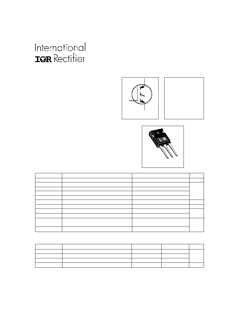
E
C
G
n-channel
Features
· Optimized for use in Welding and Switch-Mode
Power Supply applications
· Industry benchmark switching losses improve
efficiency of all power supply topologies
· 50% reduction of Eoff parameter
· Low IGBT conduction losses
· Latest technology IGBT design offers tighter
parameter distribution coupled with exceptional
reliability
· Lower switching losses allow more cost-effective
operation and hence efficient replacement of larger-
die MOSFETs up to 100kHz
· Of particular benefit in single-ended converters and
Power Supplies 150W and higher
· Reduction in critical Eoff parameter due to minimal
minority-carrier recombination coupled with low on-
state losses allow maximum flexibility in device
application
Benefits
V
CES
= 900V
V
CE(on) typ.
= 2.25V
@V
GE
= 15V, I
C
= 28A
Parameter
Max.
Units
V
CES
Collector-to-Emitter Breakdown Voltage
900
V
I
C
@ T
C
= 25°C
Continuous Collector Current
51
I
C
@ T
C
= 100°C
Continuous Collector Current
28
A
I
CM
Pulsed Collector Current
204
I
LM
Clamped Inductive Load Current
204
V
GE
Gate-to-Emitter Voltage
± 20
V
E
ARV
Reverse Voltage Avalanche Energy
186
mJ
P
D
@ T
C
= 25°C
Maximum Power Dissipation
200
P
D
@ T
C
= 100°C
Maximum Power Dissipation
78
T
J
Operating Junction and
-55 to + 150
T
STG
Storage Temperature Range
Soldering Temperature, for 10 seconds
300 (0.063 in. (1.6mm from case )
°C
Absolute Maximum Ratings
W
4/15/98
www.irf.com
1
Parameter
Typ.
Max.
Units
R
JC
Junction-to-Case
0.64
R
CS
Case-to-Sink, Flat, Greased Surface
0.24
°C/W
R
JA
Junction-to-Ambient, typical socket mount
40
Wt
Weight
6 (0.21)
g (oz)
Thermal Resistance
TO-247AC

IRG4PF50W
2
www.irf.com
Parameter
Min. Typ. Max. Units
Conditions
Q
g
Total Gate Charge (turn-on)
160
240
I
C
= 28A
Q
ge
Gate - Emitter Charge (turn-on)
19
29
nC
V
CC
= 400V
See Fig. 8
Q
gc
Gate - Collector Charge (turn-on)
53
80
V
GE
= 15V
t
d(on)
Turn-On Delay Time
29
t
r
Rise Time
26
T
J
= 25°C
t
d(off)
Turn-Off Delay Time
110
170
I
C
= 28A, V
CC
= 720V
t
f
Fall Time
150
220
V
GE
= 15V, R
G
= 5.0
E
on
Turn-On Switching Loss
0.19
Energy losses include "tail"
E
off
Turn-Off Switching Loss
1.06
mJ
See Fig. 10, 11, 13, 14
E
ts
Total Switching Loss
1.25
1.7
t
d(on)
Turn-On Delay Time
28
T
J
= 150°C,
t
r
Rise Time
26
I
C
= 28A, V
CC
= 720V
t
d(off)
Turn-Off Delay Time
280
V
GE
= 15V, R
G
= 5.0
t
f
Fall Time
90
Energy losses include "tail"
E
ts
Total Switching Loss
3.45
mJ
See Fig. 13, 14
L
E
Internal Emitter Inductance
13
nH
Measured 5mm from package
C
ies
Input Capacitance
3300
V
GE
= 0V
C
oes
Output Capacitance
200
pF
V
CC
= 30V
See Fig. 7
C
res
Reverse Transfer Capacitance
45
= 1.0MHz
Parameter
Min. Typ. Max. Units
Conditions
V
(BR)CES
Collector-to-Emitter Breakdown Voltage
900
V
V
GE
= 0V, I
C
= 250µA
V
(BR)ECS
Emitter-to-Collector Breakdown Voltage
18
V
V
GE
= 0V, I
C
= 1.0A
V
(BR)CES
/
T
J
Temperature Coeff. of Breakdown Voltage 0.295
V/°C
V
GE
= 0V, I
C
= 3.5mA
2.25
2.7
I
C
= 28A V
GE
= 15V
V
CE(ON)
Collector-to-Emitter Saturation Voltage
2.74
I
C
= 60A
See Fig.2, 5
2.12
I
C
= 28A , T
J
= 150°C
V
GE(th)
Gate Threshold Voltage
3.0
6.0
V
CE
= V
GE
, I
C
= 250µA
V
GE(th)
/
T
J
Temperature Coeff. of Threshold Voltage
-13
mV/°C V
CE
= V
GE
, I
C
= 1.0mA
g
fe
Forward Transconductance
26
39
S
V
CE
15V, I
C
= 28A
500
V
GE
= 0V, V
CE
= 900V
2.0
V
GE
= 0V, V
CE
= 10V, T
J
= 25°C
5.0
mA
V
GE
= 0V, V
CE
= 900V, T
J
= 150°C
I
GES
Gate-to-Emitter Leakage Current
±100
nA
V
GE
= ±20V
Electrical Characteristics @ T
J
= 25°C (unless otherwise specified)
I
CES
Zero Gate Voltage Collector Current
V
µ A
Switching Characteristics @ T
J
= 25°C (unless otherwise specified)
ns
ns
Pulse width
80µs; duty factor
0.1%.
Pulse width 5.0µs, single shot.
Notes:
Repetitive rating; V
GE
= 20V, pulse width limited by
max. junction temperature. ( See fig. 13b )
V
CC
= 80%(V
CES
), V
GE
= 20V, L =
10µH, R
G
= 5.0
,
(See fig. 13a)
Repetitive rating; pulse width limited by maximum
junction temperature.
IRG4PF50W
www.irf.com
3
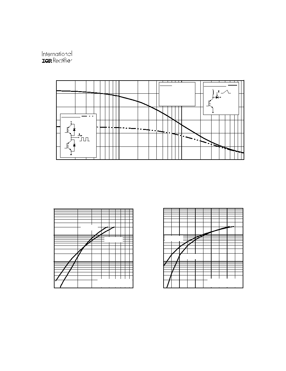
Fig. 1 - Typical Load Current vs. Frequency
(For square wave, I=I
RMS
of fundamental; for triangular wave, I=I
PK
)
Fig. 2 - Typical Output Characteristics
Fig. 3 - Typical Transfer Characteristics
1
10
100
1000
1
10
V , Collector-to-Emitter Voltage (V)
I , Collector-to-Emitter Current (A)
CE
C
V = 15V
20µs PULSE WIDTH
GE
T = 25 C
J
°
T = 150 C
J
°
1
10
100
1000
5
6
7
8
9
10
V , Gate-to-Emitter Voltage (V)
I , Collector-to-Emitter Current (A)
GE
C
V = 50V
5µs PULSE WIDTH
CC
T = 25 C
J
°
T = 150 C
J
°
0
10
20
30
40
50
60
0.1
1
10
100
f, Frequency (kHz)
)
60% of rated
voltage
Ideal diodes
Square wave:
For both:
Duty cycle: 50%
T = 125°C
T = 90°C
Gate drive as specified
sink
J
Power Dissipation = 40W
Triangular wave:
Clamp voltage:
80% of rated
Load Current ( A )
IRG4PF50W
4
www.irf.com
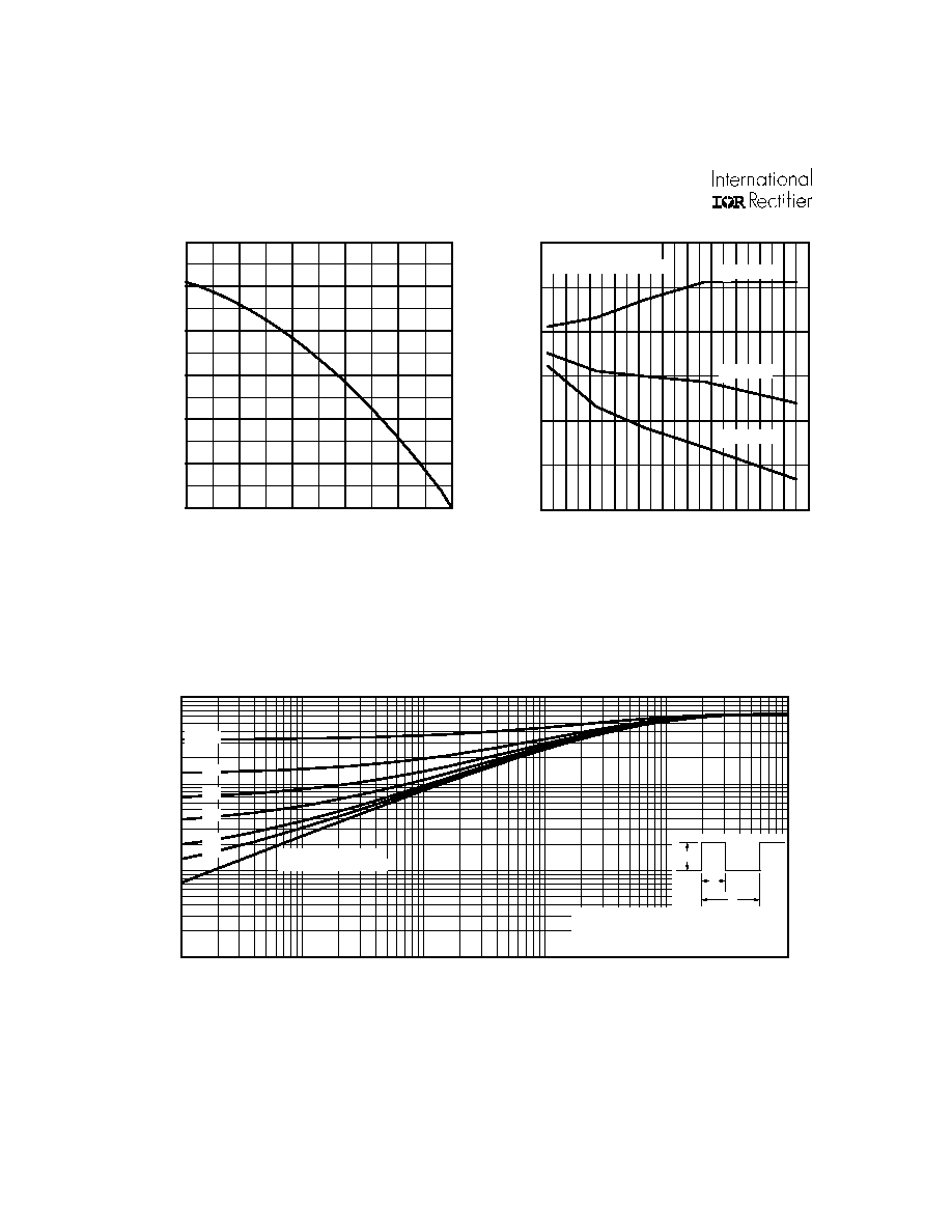
Fig. 6 - Maximum Effective Transient Thermal Impedance, Junction-to-Case
Fig. 5 - Collector-to-Emitter Voltage vs.
Junction Temperature
Fig. 4 - Maximum Collector Current vs. Case
Temperature
25
50
75
100
125
150
0
10
20
30
40
50
60
T , Case Temperature ( C)
Maximum DC Collector Current(A)
C
°
-60 -40 -20
0
20
40
60
80 100 120 140 160
1.5
2.0
2.5
3.0
T , Junction Temperature ( C)
V , Collector-to-Emitter Voltage(V)
J
°
CE
V = 15V
80 us PULSE WIDTH
GE
I = A
56
C
I = A
28
C
I = A
14
C
0.001
0.01
0.1
1
0.00001
0.0001
0.001
0.01
0.1
1
Notes:
1. Duty factor D = t / t
2. Peak T = P
x Z
+ T
1
2
J
DM
thJC
C
P
t
t
DM
1
2
t , Rectangular Pulse Duration (sec)
Thermal Response (Z )
1
thJC
0.01
0.02
0.05
0.10
0.20
D = 0.50
SINGLE PULSE
(THERMAL RESPONSE)

IRG4PF50W
www.irf.com
5
0
10
20
30
40
50
60
1.0
2.0
3.0
4.0
R , Gate Resistance
Total Switching Losses (mJ)
G
V = 720V
V = 15V
T = 25 C
I = 28A
CC
GE
J
C
°
Fig. 10 - Typical Switching Losses vs.
Junction Temperature
Fig. 9 - Typical Switching Losses vs. Gate
Resistance
Fig. 8 - Typical Gate Charge vs.
Gate-to-Emitter Voltage
Fig. 7 - Typical Capacitance vs.
Collector-to-Emitter Voltage
(
)
0
40
80
120
160
0
4
8
12
16
20
Q , Total Gate Charge (nC)
V , Gate-to-Emitter Voltage (V)
G
GE
V
= 400V
I
= 28A
CC
C
1
10
100
0
1000
2000
3000
4000
5000
6000
V , Collector-to-Emitter Voltage (V)
C, Capacitance (pF)
CE
V
C
C
C
=
=
=
=
0V,
C
C
C
f = 1MHz
+ C
+ C
C SHORTED
GE
ies
ge
gc ,
ce
res
gc
oes
ce
gc
C
ies
C
oes
C
res
-60 -40 -20
0
20
40
60
80 100 120 140 160
0.1
1
10
100
T , Junction Temperature ( C )
Total Switching Losses (mJ)
J
°
R = Ohm
V = 15V
V = 720V
G
GE
CC
I = A
56
C
I = A
28
C
I = A
14
C
5.0