IRG4PC50S-P.p65
Parameter
Max.
Units
V
CES
Collector-to-Emitter Breakdown Voltage
600
V
I
C
@ T
C
= 25°C
Continuous Collector Current
70
I
C
@ T
C
= 100°C
Continuous Collector Current
41
A
I
CM
Pulsed Collector Current
Q
140
I
LM
Clamped Inductive Load Current
R
140
V
GE
Gate-to-Emitter Voltage
± 20
V
E
ARV
Reverse Voltage Avalanche Energy
S
20
mJ
P
D
@ T
C
= 25°C
Maximum Power Dissipation
200
P
D
@ T
C
= 100°C
Maximum Power Dissipation
78
T
J
Operating Junction and
-55 to + 150
T
STG
Storage Temperature Range
°C
Max Reflow Temperature
225
IRG4PC50S-P
Standard Speed IGBT
INSULATED GATE BIPOLAR TRANSISTOR
Parameter
Typ.
Max.
Units
R
JC
Junction-to-Case
0.64
R
CS
Case-to-Sink, Flat, Greased Surface
0.24
°C/W
R
JA
Junction-to-Ambient, typical socket mount
40
Thermal Resistance
Absolute Maximum Ratings
W
E
C
G
n-channel
Features
Features
Features
Features
Features
· Standard: Optimized for minimum saturation
voltage and low operating frequencies ( < 1kHz)
· Generation 4 IGBT design provides tighter
parameter distribution and higher efficiency than
Generation 3
· Industry standard TO-247AC package
· Surface Mountable
· Generation 4 IGBT's offer highest efficiency available
· IGBT's optimized for specified application conditions
· Designed to be a "drop-in" replacement for equivalent
industry-standard Generation 3 IR IGBT's
Benefits
V
CES
= 600V
V
CE(on) typ.
=
1.28V
@V
GE
= 15V, I
C
= 41A
1
www.irf.com
05/14/02
Surface Mountable
TO-247
PD - 91581B
IRG4PC50S-P
2
www.irf.com
Parameter
Min. Typ. Max. Units
Conditions
Q
g
Total Gate Charge (turn-on)
--
180
280
I
C
= 41A
Q
ge
Gate - Emitter Charge (turn-on)
--
24
37
nC
V
CC
= 400V
See Fig. 8
Q
gc
Gate - Collector Charge (turn-on)
--
61
92
V
GE
= 15V
t
d(on)
Turn-On Delay Time
--
33
--
t
r
Rise Time
--
30
--
T
J
= 25°C
t
d(off)
Turn-Off Delay Time
--
650
980
I
C
= 41A, V
CC
= 480V
t
f
Fall Time
--
400
600
V
GE
= 15V, R
G
= 5.0
E
on
Turn-On Switching Loss
--
0.72
--
Energy losses include "tail"
E
off
Turn-Off Switching Loss
--
8.27
--
mJ
See Fig. 9, 10, 14
E
ts
Total Switching Loss
--
8.99
13
t
d(on)
Turn-On Delay Time
--
31
--
T
J
= 150°C,
t
r
Rise Time
--
31
--
I
C
= 41A, V
CC
= 480V
t
d(off)
Turn-Off Delay Time
--
1080
--
V
GE
= 15V, R
G
= 5.0
t
f
Fall Time
--
620
--
Energy losses include "tail"
E
ts
Total Switching Loss
--
15
--
mJ
See Fig. 11, 14
L
E
Internal Emitter Inductance
--
13
--
nH
Measured 5mm from package
C
ies
Input Capacitance
--
4100
--
V
GE
= 0V
C
oes
Output Capacitance
--
250
--
pF
V
CC
= 30V
See Fig. 7
C
res
Reverse Transfer Capacitance
--
48
--
= 1.0MHz
Parameter
Min. Typ. Max. Units
Conditions
V
(BR)CES
Collector-to-Emitter Breakdown Voltage
600
--
--
V
V
GE
= 0V, I
C
= 250µA
V
(BR)ECS
Emitter-to-Collector Breakdown Voltage
T
18
--
--
V
V
GE
= 0V, I
C
= 1.0A
V
(BR)CES
/
T
J
Temperature Coeff. of Breakdown Voltage
--
0.75
--
V/°C
V
GE
= 0V, I
C
= 1.0mA
--
1.28
1.36
I
C
= 41A V
GE
= 15V
V
CE(ON)
Collector-to-Emitter Saturation Voltage
--
1.62
--
I
C
= 80A
See Fig.2, 5
--
1.28
--
I
C
= 41A , T
J
= 150°C
V
GE(th)
Gate Threshold Voltage
3.0
--
6.0
V
CE
= V
GE
, I
C
= 250µA
V
GE(th)
/
T
J
Temperature Coeff. of Threshold Voltage
--
-9.3
--
mV/°C V
CE
= V
GE
, I
C
= 250µA
g
fe
Forward Transconductance
U
17
34
--
S
V
CE
=
100V, I
C
= 41A
--
--
250
V
GE
= 0V, V
CE
= 600V
--
--
2.0
V
GE
= 0V, V
CE
= 10V, T
J
= 25°C
--
--
1000
V
GE
= 0V, V
CE
= 600V, T
J
= 150°C
I
GES
Gate-to-Emitter Leakage Current
--
--
±100
nA
V
GE
= ±20V
Electrical Characteristics @ T
J
= 25°C (unless otherwise specified)
I
CES
Zero Gate Voltage Collector Current
V
µA
Switching Characteristics @ T
J
= 25°C (unless otherwise specified)
ns
ns
T
Pulse width
80µs; duty factor
0.1%.
U
Pulse width 5.0µs, single shot.
Notes:
Q
Repetitive rating; V
GE
= 20V, pulse width limited by
max. junction temperature. ( See fig. 13b )
R
V
CC
= 80%(V
CES
), V
GE
= 20V, L = 10µH, R
G
= 5.0
,
(See fig. 13a)
S
Repetitive rating; pulse width limited by maximum
junction temperature.
IRG4PC50S-P
www.irf.com
3
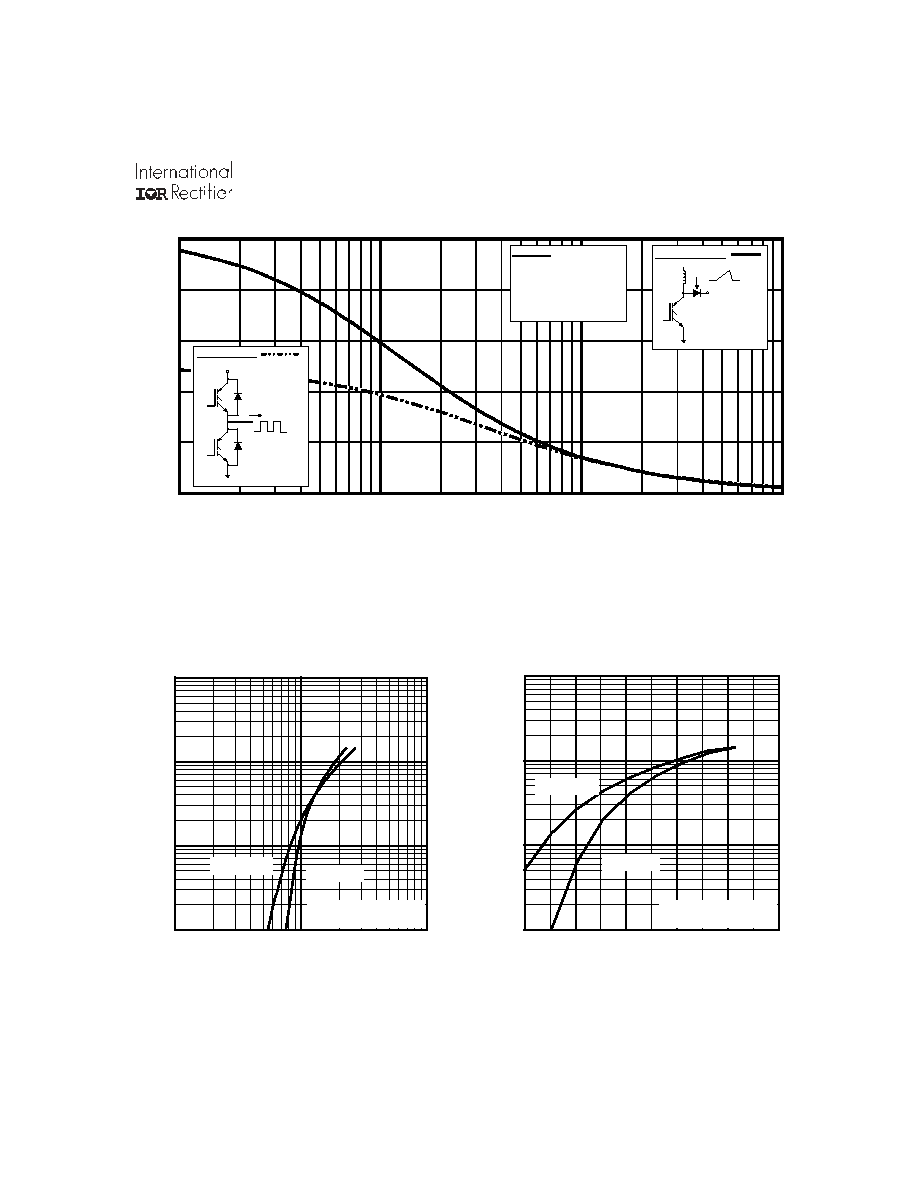
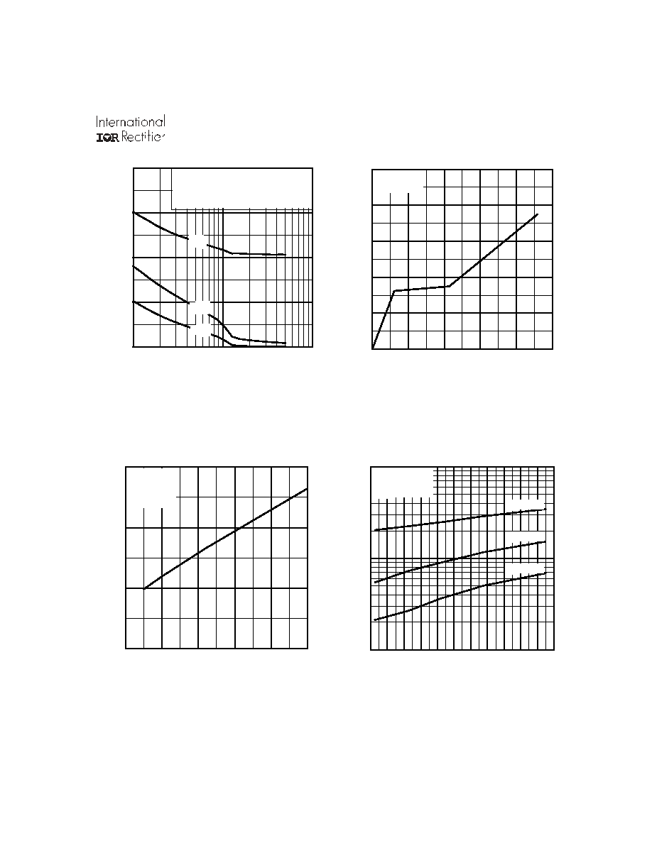
Fig. 1 - Typical Load Current vs. Frequency
(Load Current = I
RMS
of fundamental)
Fig. 2 - Typical Output Characteristics
Fig. 3 - Typical Transfer Characteristics
1
10
100
1000
0.1
1
10
V , Collector-to-Emitter Voltage (V)
I , Collector-to-Emitter Current (A)
CE
C
V = 15V
20µs PULSE WIDTH
GE
T = 25 C
J
o
T = 150 C
J
o
1
10
100
1000
5
6
7
8
9
10
V , Gate-to-Emitter Voltage (V)
I , Collector-to-Emitter Current (A)
GE
C
V = 50V
5µs PULSE WIDTH
CC
T = 25 C
J
o
T = 150 C
J
o
0
2 0
4 0
6 0
8 0
1 0 0
0 . 1
1
1 0
1 0 0
f, Frequency (kHz)
A
6 0 % o f ra te d
vo lt a g e
I
Id e a l di o de s
S q u are wa ve:
F o r b o t h :
D uty cy c le : 5 0%
T = 12 5° C
T = 90 °C
G a te d rive a s s pe c ified
s in k
J
P o w e r D i ss i p a tio n = 4 0 W
T ria n g u la r wa v e :
I
C la m p v o lt a g e :
8 0 % o f r a t e d
Load Current ( A )
IRG4PC50S-P
4
www.irf.com
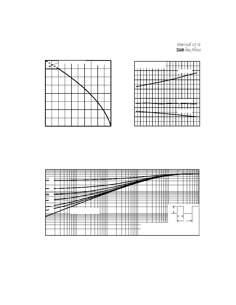
Fig. 6 - Maximum Effective Transient Thermal Impedance, Junction-to-Case
Fig. 5 - Typical Collector-to-Emitter Voltage
vs. Junction Temperature
Fig. 4 - Maximum Collector Current vs. Case
Temperature
-60 -40 -20
0
20
40
60
80 100 120 140 160
0.8
1.0
1.2
1.4
1.6
1.8
2.0
2.2
T , Junction Temperature ( C)
V , Collector-to-Emitter Voltage(V)
J
°
CE
V = 15V
80 us PULSE WIDTH
GE
I = A
20.5
C
I = A
41
C
I = A
82
C
0
2 0
4 0
6 0
8 0
2 5
5 0
7 5
1 0 0
1 2 5
1 5 0
M
a
x
i
m
u
m
DC Co
l
l
e
c
t
o
r
Cu
r
r
e
n
t
(
A
)
T , C ase Tem perature (°C )
C
V = 15 V
G E
L IM IT E D B Y P A C K A G E
0.001
0.01
0.1
1
0.00001
0.0001
0.001
0.01
0.1
1
Notes:
1. Duty factor D = t / t
2. Peak T = P
x Z
+ T
1
2
J
DM
thJC
C
P
t
t
DM
1
2
t , Rectangular Pulse Duration (sec)
Thermal Response (Z )
1
thJC
0.01
0.02
0.05
0.10
0.20
0.50
SINGLE PULSE
(THERMAL RESPONSE)
IRG4PC50S-P
www.irf.com
5
Fig. 7 - Typical Capacitance vs.
Collector-to-Emitter Voltage
Fig. 8 - Typical Gate Charge vs.
Gate-to-Emitter Voltage
Fig. 9 - Typical Switching Losses vs. Gate
Resistance
Fig. 10 - Typical Switching Losses vs.
Junction Temperature
0
40
80
120
160
200
0
4
8
12
16
20
Q , Total Gate Charge (nC)
V , Gate-to-Emitter Voltage (V)
G
GE
V
= 400V
I
= 41A
CC
C
-60 -40 -20
0
20
40
60
80 100 120 140 160
1
10
100
T , Junction Temperature ( C )
Total Switching Losses (mJ)
J
°
R = Ohm
V = 15V
V = 480V
G
GE
CC
I = A
82
C
I = A
41
C
I = A
20.5
C
5.0
1
10
100
0
2000
4000
6000
8000
V , Collector-to-Emitter Voltage (V)
C, Capacitance (pF)
CE
V
C
C
C
=
=
=
=
0V,
C
C
C
f = 1MHz
+ C
+ C
C SHORTED
GE
ies
ge
gc ,
ce
res
gc
oes
ce
gc
Cies
Coes
Cres
0
10
20
30
40
50
8.5
9.0
9.5
10.0
R , Gate Resistance (Ohm)
Total Switching Losses (mJ)
G
V = 480V
V = 15V
T = 25 C
I = 41A
CC
GE
J
C
°
R
G
, Gate Resistance
( )