Äîêóìåíòàöèÿ è îïèñàíèÿ www.docs.chipfind.ru
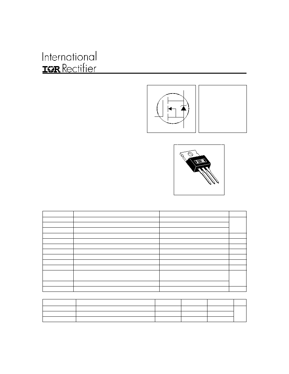
IRFZ34E
HEXFET
®
Power MOSFET
PD - 9.1672A
V
DSS
= 60V
R
DS(on)
= 0.042
I
D
= 28A
l
Advanced Process Technology
l
Ultra Low On-Resistance
l
Dynamic dv/dt Rating
l
175°C Operating Temperature
l
Fast Switching
l
Ease of Paralleling
Thermal Resistance
Fifth Generation HEXFETs from International Rectifier
utilize advanced processing techniques to achieve
the lowest possible on-resistance per silicon area.
This benefit, combined with the fast switching speed
and ruggedized device design that HEXFET Power
MOSFETs are well known for, provides the designer
with an extremely efficient device for use in a wide
variety of applications.
The TO-220 package is universally preferred for all
commercial-industrial applications at power dissipation
levels to approximately 50 watts. The low thermal
resistance and low package cost of the TO-220
contribute to its wide acceptance throughout the
industry.
Description
Parameter
Min.
Typ.
Max.
Units
R
JC
Junction-to-Case
2.2
R
CS
Case-to-Sink, Flat, Greased Surface
0.50
°C/W
R
JA
Junction-to-Ambient
62
TO-220AB
S
D
G
11/4/97
Parameter
Max.
Units
I
D
@ T
C
= 25°C
Continuous Drain Current, V
GS
@ 10V
28
I
D
@ T
C
= 100°C
Continuous Drain Current, V
GS
@ 10V
20
A
I
DM
Pulsed Drain Current
112
P
D
@T
C
= 25°C
Power Dissipation
68
W
Linear Derating Factor
0.46
W/°C
V
GS
Gate-to-Source Voltage
± 20
V
E
AS
Single Pulse Avalanche Energy
97
mJ
I
AR
Avalanche Current
17
A
E
AR
Repetitive Avalanche Energy
6.8
mJ
dv/dt
Peak Diode Recovery dv/dt
5.0
V/ns
T
J
Operating Junction and
-55 to + 175
T
STG
Storage Temperature Range
Soldering Temperature, for 10 seconds
300 (1.6mm from case )
°C
Mounting torque, 6-32 or M3 srew
10 lbf·in (1.1N·m)
Absolute Maximum Ratings
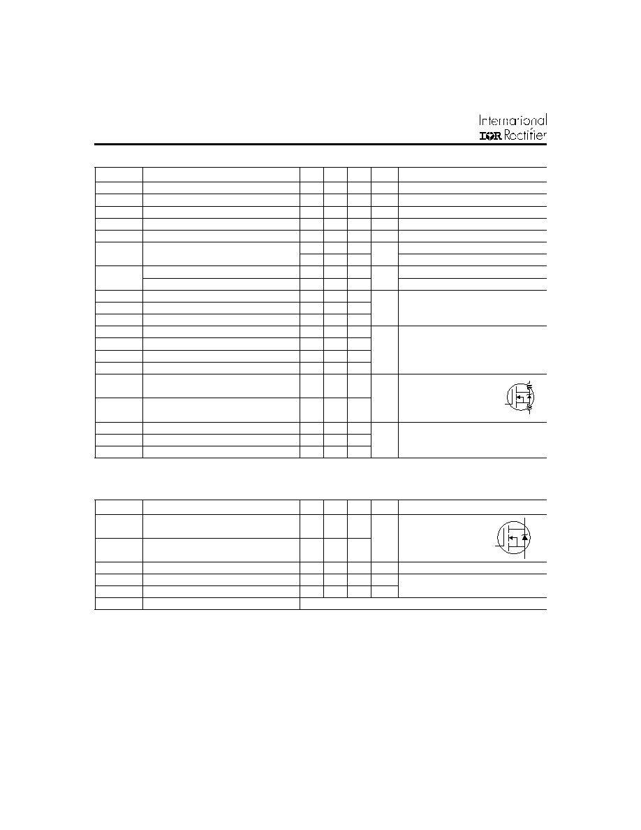
IRFZ34E
Notes:
Parameter
Min. Typ. Max. Units
Conditions
I
S
Continuous Source Current
MOSFET symbol
(Body Diode)
showing the
I
SM
Pulsed Source Current
integral reverse
(Body Diode)
p-n junction diode.
V
SD
Diode Forward Voltage
1.3
V
T
J
= 25°C, I
S
= 17A, V
GS
= 0V
t
rr
Reverse Recovery Time
63
95
ns
T
J
= 25°C, I
F
= 17A
Q
rr
Reverse Recovery Charge
130
200
nC
di/dt = 100A/µs
t
on
Forward Turn-On Time
Repetitive rating; pulse width limited by
max. junction temperature. ( See fig. 11 )
Starting T
J
= 25°C, L = 670µH
R
G
= 25
, I
AS
= 17A. (See Figure 12)
I
SD
17 A, di/dt
200A/µs, V
DD
V
(BR)DSS
,
T
J
175°C
Pulse width
300µs; duty cycle
2%.
Source-Drain Ratings and Characteristics
Electrical Characteristics @ T
J
= 25°C (unless otherwise specified)
Parameter
Min. Typ. Max. Units
Conditions
V
(BR)DSS
Drain-to-Source Breakdown Voltage
60
V
V
GS
= 0V, I
D
= 250µA
V
(BR)DSS
/
T
J
Breakdown Voltage Temp. Coefficient
0.056
V/°C
Reference to 25°C, I
D
= 1mA
R
DS(ON)
Static Drain-to-Source On-Resistance
0.042
V
GS
= 10V, I
D
= 17A
V
GS(th)
Gate Threshold Voltage
2.0
4.0
V
V
DS
= V
GS
, I
D
= 250µA
g
fs
Forward Transconductance
7.6
S
V
DS
= 25V, I
D
= 17A
25
V
DS
= 60V, V
GS
= 0V
250
V
DS
= 48V, V
GS
= 0V, T
J
= 150°C
Gate-to-Source Forward Leakage
100
V
GS
= 20V
Gate-to-Source Reverse Leakage
-100
V
GS
= -20V
Q
g
Total Gate Charge
30
I
D
= 17A
Q
gs
Gate-to-Source Charge
6.7
nC
V
DS
= 48V
Q
gd
Gate-to-Drain ("Miller") Charge
12
V
GS
= 10V, See Fig. 6 and 13
t
d(on)
Turn-On Delay Time
5.1
V
DD
= 30V
t
r
Rise Time
30
I
D
= 17A
t
d(off)
Turn-Off Delay Time
22
R
G
= 13
t
f
Fall Time
30
R
D
= 1.8
,
See Fig. 10
Between lead,
6mm (0.25in.)
from package
and center of die contact
C
iss
Input Capacitance
680
V
GS
= 0V
C
oss
Output Capacitance
220
pF
V
DS
= 25V
C
rss
Reverse Transfer Capacitance
80
= 1.0MHz, See Fig. 5
Intrinsic turn-on time is negligible (turn-on is dominated by L
S
+L
D
)
100
28
A
nH
L
D
Internal Drain Inductance
4.5
L
S
Internal Source Inductance
7.5
I
DSS
Drain-to-Source Leakage Current
I
GSS
ns
µA
nA
S
D
G
S
D
G
IRFZ34E
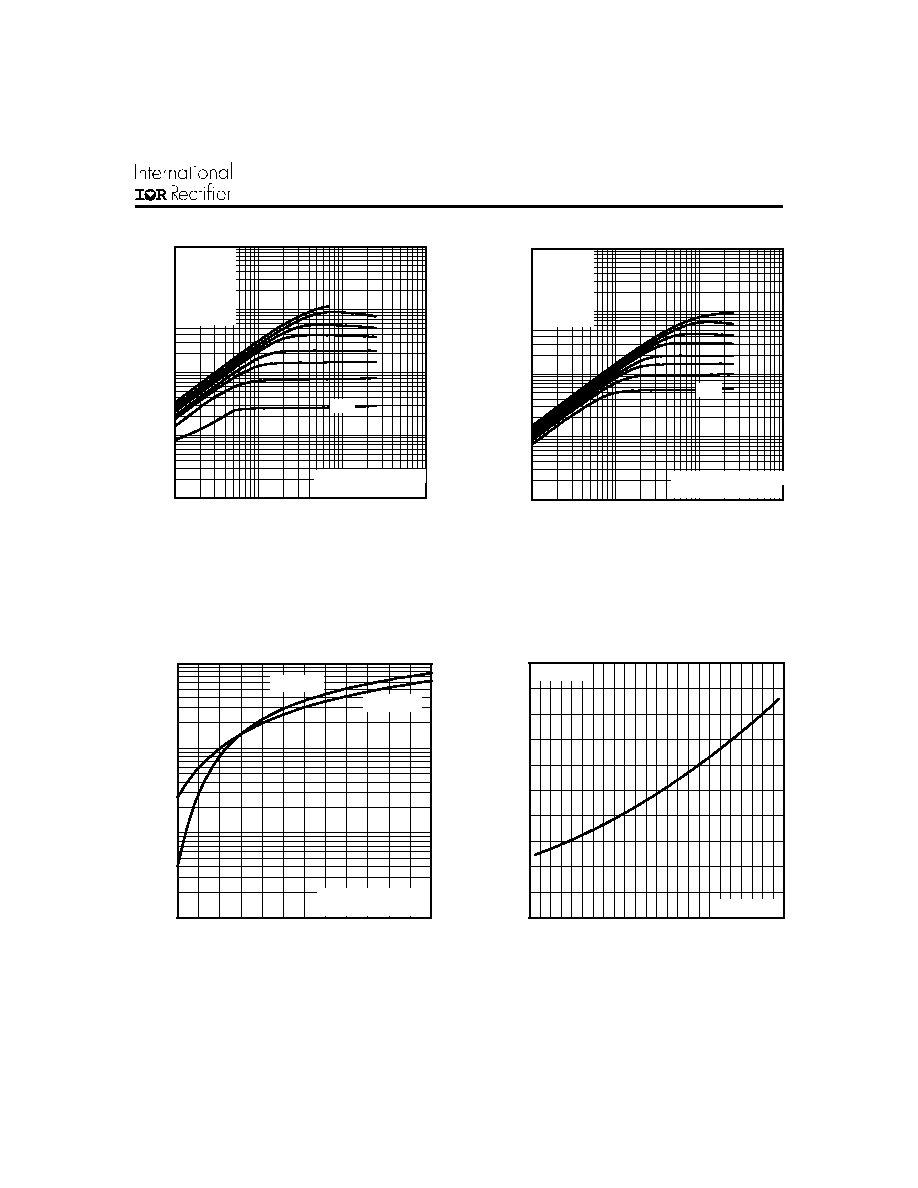
Fig 3. Typical Transfer Characteristics
Fig 4. Normalized On-Resistance
Vs. Temperature
Fig 1. Typical Output Characteristics
Fig 2. Typical Output Characteristics
0.1
1
10
100
1000
0.1
1
10
100
20µs PULSE WIDTH
T = 25 C
J
°
TOP
BOTTOM
VGS
15V
10V
8.0V
7.0V
6.0V
5.5V
5.0V
4.5V
V , Drain-to-Source Voltage (V)
I , Drain-to-Source Current (A)
DS
D
4.5V
0.1
1
10
100
1000
0.1
1
10
100
20µs PULSE WIDTH
T = 175 C
J
°
TOP
BOTTOM
VGS
15V
10V
8.0V
7.0V
6.0V
5.5V
5.0V
4.5V
V , Drain-to-Source Voltage (V)
I , Drain-to-Source Current (A)
DS
D
4.5V
0.1
1
10
100
4
5
6
7
8
9
10
V = 25V
20µs PULSE WIDTH
DS
V , Gate-to-Source Voltage (V)
I , Drain-to-Source Current (A)
GS
D
T = 175 C
J
°
T = 25 C
J
°
-60 -40 -20
0
20 40 60 80 100 120 140 160 180
0.0
0.5
1.0
1.5
2.0
2.5
T , Junction Temperature( C)
R , Drain-to-Source On Resistance
(Normalized)
J
DS(on)
°
V
=
I =
GS
D
10V
28A
IRFZ34E
1
10
100
1000
1
10
100
1000
OPERATION IN THIS AREA LIMITED
BY R
DS(on)
Single Pulse
T
T
= 175 C
= 25 C
°
°
J
C
V , Drain-to-Source Voltage (V)
I , Drain Current (A)
I , Drain Current (A)
DS
D
10us
100us
1ms
10ms
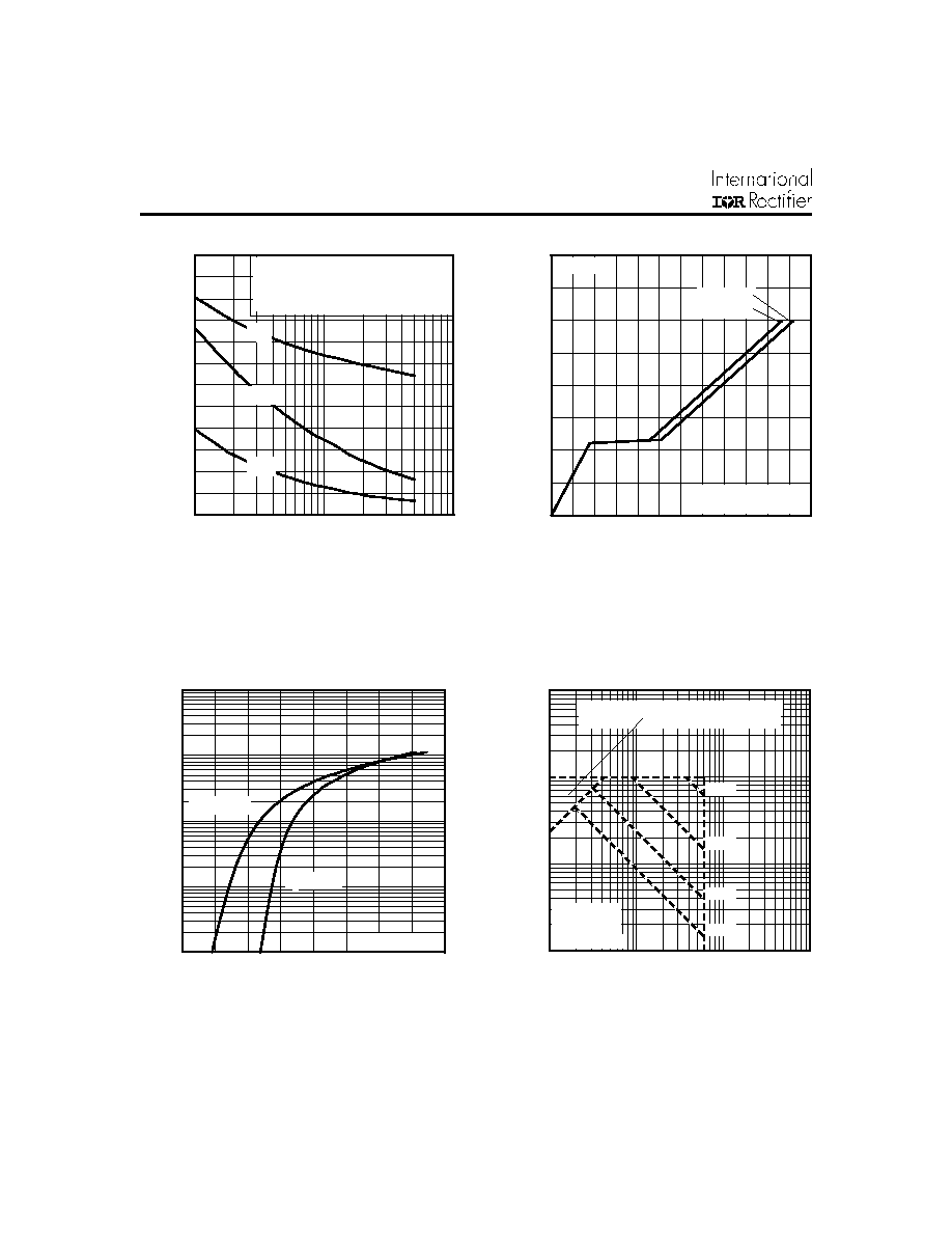
Fig 7. Typical Source-Drain Diode
Forward Voltage
Fig 8. Maximum Safe Operating Area
Fig 5. Typical Capacitance Vs.
Drain-to-Source Voltage
Fig 6. Typical Gate Charge Vs.
Gate-to-Source Voltage
1
10
100
0
200
400
600
800
1000
1200
V , Drain-to-Source Voltage (V)
C, Capacitance (pF)
DS
V
C
C
C
=
=
=
=
0V,
C
C
C
f = 1MHz
+ C
+ C
C SHORTED
GS
iss
gs
gd ,
ds
rss
gd
oss
ds
gd
Ciss
Coss
Crss
0.1
1
10
100
1000
0.2
0.6
1.0
1.4
1.8
V ,Source-to-Drain Voltage (V)
I , Reverse Drain Current (A)
SD
SD
V = 0 V
GS
T = 25 C
J
°
T = 150 C
J
°
0
5
10
15
20
25
30
0
5
10
15
20
Q , Total Gate Charge (nC)
V , Gate-to-Source Voltage (V)
G
GS
FOR TEST CIRCUIT
SEE FIGURE
I =
D
13
17 A
V
= 30V
DS
V
= 48V
DS
IRFZ34E
Fig 10a. Switching Time Test Circuit
+
-
V
DS
90%
10%
V
GS
t
d(on)
t
r
t
d(off)
t
f
V
DS
10 V
Pulse Width
1
µs
Duty Factor
0.1 %
Fig 9. Maximum Drain Current Vs.
Case Temperature
Fig 10b. Switching Time Waveforms
R
D
V
GS
V
DD
R
G
D.U.T.
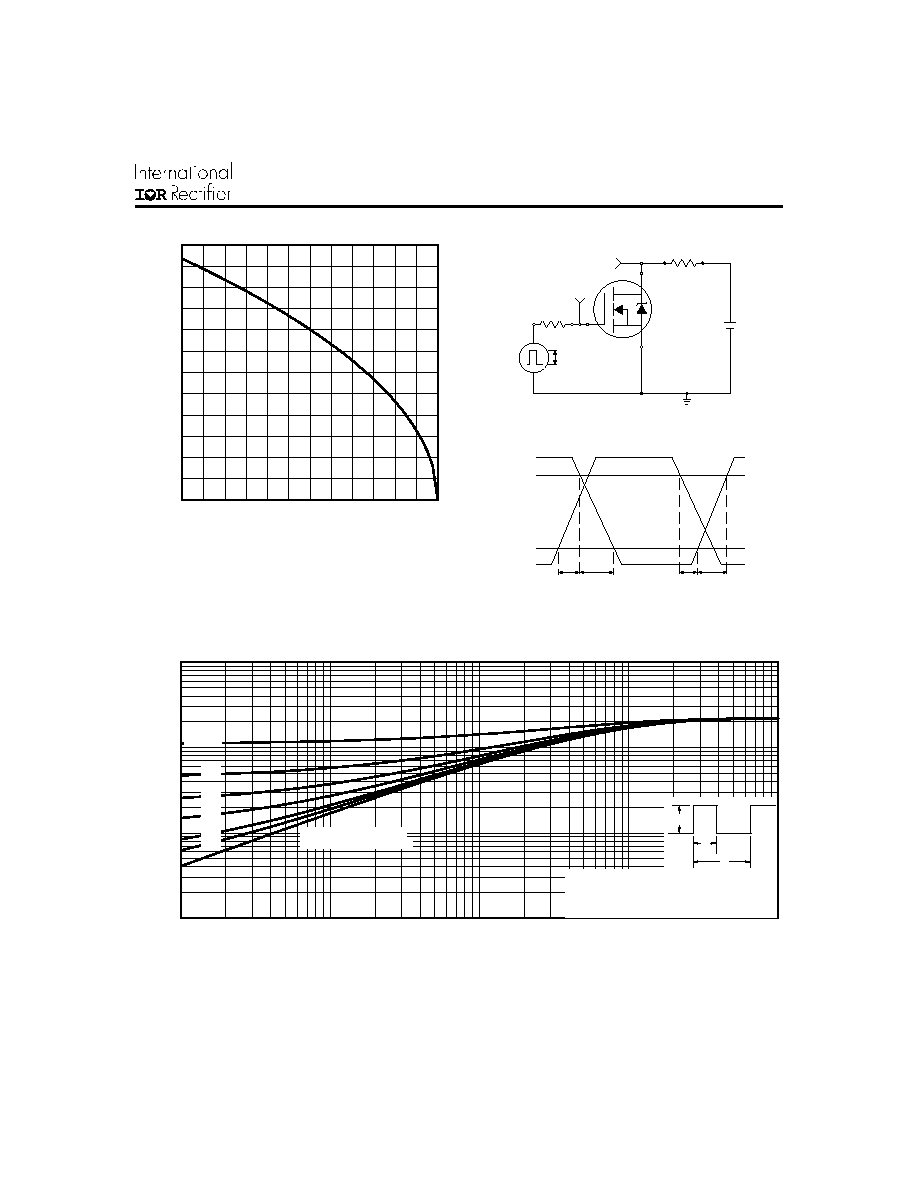
Fig 11. Maximum Effective Transient Thermal Impedance, Junction-to-Case
25
50
75
100
125
150
175
0
5
10
15
20
25
30
T , Case Temperature ( C)
I , Drain Current (A)
°
C
D
0.01
0.1
1
10
0.00001
0.0001
0.001
0.01
0.1
Notes:
1. Duty factor D = t / t
2. Peak T = P
x Z
+ T
1
2
J
DM
thJC
C
P
t
t
DM
1
2
t , Rectangular Pulse Duration (sec)
Thermal Response
(Z )
1
thJC
0.01
0.02
0.05
0.10
0.20
D = 0.50
SINGLE PULSE
(THERMAL RESPONSE)