IRFPC60LC-P
HEXFET
®
Power MOSFET
PD - 99438
S
D
G
V
DSS
= 600V
R
DS(on)
= 0.40
I
D
= 16A
l
Ultra Low Gate Charge
l
Reduced Gate Drive Requirement
l
Enhanced 30V V
gs
Rating
l
Reduced C
iss
, C
oss
, C
rss
l
Isolated Central Mounting Hole
l
Dynamic dv/dt Rated
l
Repetitive Avalanche Rated
Absolute Maximum Ratings
Parameter
Max.
Units
I
D
@ T
C
= 25°C
Continuous Drain Current, V
GS
@ 10V
16
I
D
@ T
C
= 100°C
Continuous Drain Current, V
GS
@ 10V
10
A
I
DM
Pulsed Drain Current
64
P
D
@T
C
= 25°C
Power Dissipation
280
W
Linear Derating Factor
2.2
W/°C
V
GS
Gate-to-Source Voltage
±30
V
E
AS
Single Pulse Avalanche Energy
1000
mJ
I
AR
Avalanche Current
16
A
E
AR
Repetitive Avalanche Energy
28
mJ
dv/dt
Peak Diode Recovery dv/dt
3.0
V/ns
T
J
Operating Junction and
-55 to + 150
T
STG
Storage Temperature Range
°C
Max Reflow Temperature
225
Parameter
Min.
Typ.
Max.
Units
R
JC
Junction-to-Case
0.45
R
CS
Case-to-Sink, Flat, Greased Surface
0.24
°C/W
R
JA
Junction-to-Ambient
40
Thermal Resistance
Description
This new series of Surface Mountable Low Charge HEXFET Power MOSFETs
achieve significantly lower gate charge over conventional MOSFETs. Utilizing
advanced Hexfet technology the device improvements allow for reduced gate
drive requirements, faster switching speeds and increased total system savings.
These device improvements combined with the proven ruggedness and reliability
of HEXFETs offer the designer a new standard in power transistors for switching
applications.
www.irf.com
1
04/25/02
Surface Mountable
TO-247
2
www.irf.com
IRFPC60LC-P
Notes:
Parameter
Min. Typ. Max. Units
Conditions
I
S
Continuous Source Current
MOSFET symbol
(Body Diode)
showing the
I
SM
Pulsed Source Current
integral reverse
(Body Diode)
p-n junction diode.
V
SD
Diode Forward Voltage
1.8
V
T
J
= 25°C, I
S
= 16A, V
GS
= 0V
t
rr
Reverse Recovery Time
650
980
ns
T
J
= 25°C, I
F
= 16A
Q
rr
Reverse RecoveryCharge
6.0
9.0
µC
di/dt = 100A/µs
t
on
Forward Turn-On Time
Repetitive rating; pulse width limited by
max. junction temperature. ( See fig. 11 )
V
DD
= 25V, starting T
J
= 25°C, L = 7.2mH
R
G
= 25
, I
AS
= 16A. (See Figure 12)
I
SD
16A, di/dt
140A/µs, V
DD
V
(BR)DSS
,
T
J
150°C
Pulse width
300µs; duty cycle
2%.
Source-Drain Ratings and Characteristics
Electrical Characteristics @ T
J
= 25°C (unless otherwise specified)
Parameter
Min. Typ. Max. Units
Conditions
V
(BR)DSS
Drain-to-Source Breakdown Voltage
600
V
V
GS
= 0V, ID = 250µA
V
(BR)DSS
/
T
J
Breakdown Voltage Temp. Coefficient
0.63
V/°C
Reference to 25°C, I
D
= 1mA
R
DS(ON)
Static Drain-to-Source On-Resistance
0.40
V
GS
= 10V, I
D
= 9.6A
V
GS(th)
Gate Threshold Voltage
2.0
4.0
V
V
DS
= V
GS
, I
D
= 250µA
g
fs
Forward Transconductance
11
S
V
DS
= 50V, I
D
= 9.6A
25
V
DS
= 600V, V
GS
= 0V
250
V
DS
= 480V, V
GS
= 0V, T
J
= 125°C
Gate-to-Source Forward Leakage
100
V
GS
= 20V
Gate-to-Source Reverse Leakage
-100
V
GS
= -20V
Q
g
Total Gate Charge
120
I
D
= 16A
Q
gs
Gate-to-Source Charge
29
nC
V
DS
= 360V
Q
gd
Gate-to-Drain ("Miller") Charge
48
V
GS
= 10V, See Fig. 6 and 13
t
d(on)
Turn-On Delay Time
17
V
DD
= 300V
t
r
Rise Time
57
I
D
= 16A
t
d(off)
Turn-Off Delay Time
43
R
G
= 4.3
t
f
Fall Time
38
R
D
= 18
,
See Fig. 10
Between lead,
6mm (0.25in.)
from package
and center of die contact
C
iss
Input Capacitance
3500
V
GS
= 0V
C
oss
Output Capacitance
400
pF
V
DS
= 25V
C
rss
Reverse Transfer Capacitance
39
= 1.0MHz, See Fig. 5
Intrinsic turn-on time is negligible (turn-on is dominated by L
S
+L
D
)
64
16
A
nH
L
D
Internal Drain Inductance
5.0
L
S
Internal Source Inductance
13
I
DSS
Drain-to-Source Leakage Current
I
GSS
ns
µA
nA
S
D
G
S
D
G

www.irf.com
3
IRFPC60LC-P
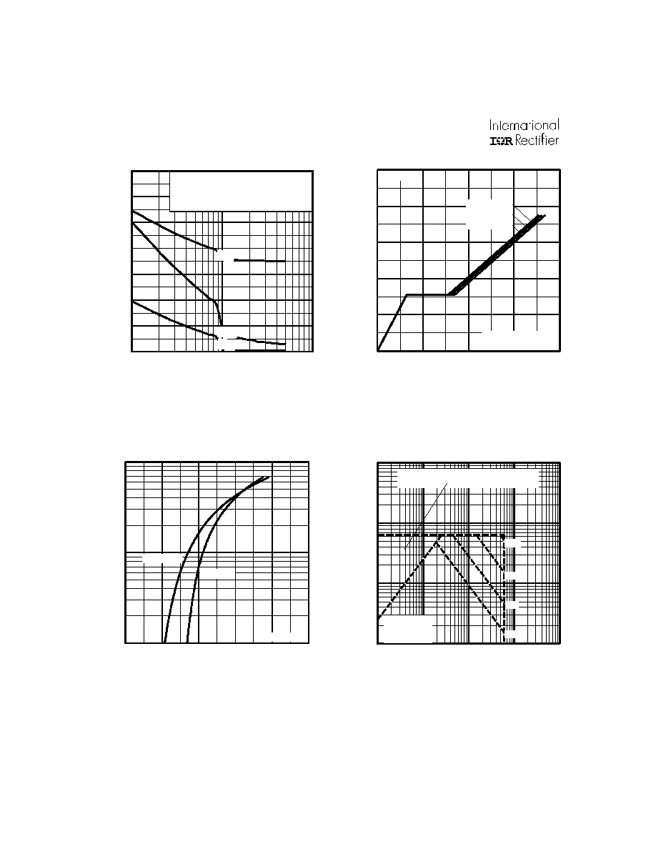
Fig 3. Typical Transfer Characteristics
Fig 4. Normalized On-Resistance
Vs. Temperature
Fig 1. Typical Output Characteristics,
T
C
= 25
o
C
Fig 2. Typical Output Characteristics,
T
C
= 150
o
C
0 .0 1
0 .1
1
1 0
1 0 0
4
5
6
7
8
9
1 0
T = 25 °C
T = 1 50°C
J
J
G S
V , G ate-to-S ourc e V o ltag e (V )
V = 1 00 V
2 0µ s P U L S E W ID T H
D
I , D
r
a
i
n
-
to
-
S
o
u
r
c
e
C
u
r
r
e
n
t
(
A
)
D S
0 .0
0 .5
1 .0
1 .5
2 .0
2 .5
3 .0
-6 0
-4 0
-2 0
0
2 0
4 0
6 0
8 0
1 0 0 1 2 0 1 4 0 1 6 0
V = 10V
G S
J
T , Ju n ctio n Te m p e ra tu re (°C )
R
,
D
r
a
i
n
-
to
-
S
o
u
r
c
e
O
n
R
e
s
i
s
t
a
n
c
e
DS
(
o
n
)
(
N
o
r
m
a
liz
e
d
)
I = 1 6 A
D
0 .0 1
0 .1
1
1 0
1 0 0
0 .0 1
0 .1
1
1 0
1 0 0
4 .5V
VGS
TOP 15V
10V
8.0V
7.0V
6.0V
5.5V
5.0V
BOTTOM 4.5V
I
,
D
r
ai
n-
t
o
-
S
our
c
e
C
u
r
r
ent
(
A
)
D
V , D ra in -to -So urce Vo lta g e (V)
D S
2 0µ s P U L S E W ID T H
T = 25 °C
C
0 .0 1
0 .1
1
1 0
1 0 0
0 .0 1
0 .1
1
1 0
1 0 0
VGS
TOP 15V
10V
8.0V
7.0V
6.0V
5.5V
5.0V
BOTTOM 4.5V
I
,
D
r
ai
n-
t
o
-
S
our
c
e
C
u
r
r
ent
(
A
)
D
V , D ra in -to -So urce Vo lta g e (V)
D S
20 µ s P U LS E W ID T H
T = 150 °C
C
4 .5V
4
www.irf.com
IRFPC60LC-P
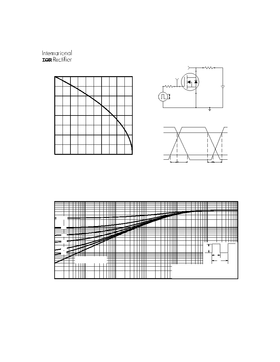
Fig 7. Typical Source-Drain Diode
Forward Voltage
Fig 8. Maximum Safe Operating Area
Fig 5. Typical Capacitance Vs.
Drain-to-Source Voltage
Fig 6. Typical Gate Charge Vs.
Gate-to-Source Voltage
0
1 00 0
2 00 0
3 00 0
4 00 0
5 00 0
6 00 0
7 00 0
1
1 0
1 00
C
,
C
apac
i
t
an
c
e
(
p
F
)
D S
V , D ra in -to -S o u rce V o lta g e (V )
V = 0 V , f = 1 M H z
C = C + C , C S H O R T E D
C = C
C = C + C
G S
is s gs g d d s
rs s g d
o s s d s g d
C
is s
C
o ss
C
rs s
0
4
8
1 2
1 6
2 0
0
3 0
60
9 0
12 0
Q , T ota l G ate C h a rg e (n C )
G
F O R T E S T C IR C U IT
S E E F IG U R E 13
V
,
G
a
t
e
-
t
o-
S
our
c
e
V
o
l
t
age (
V
)
GS
I = 1 6A
D
V = 3 60 V
V = 2 40 V
V = 1 20 V
D S
D S
D S
1
1 0
1 0 0
0
0 .4
0 .8
1 .2
1 .6
2
T = 25 °C
T = 1 50 °C
J
J
V = 0 V
G S
V , So u rce -to -D ra in V o lta g e (V)
I , R
e
v
e
r
s
e
D
r
a
i
n
C
u
r
r
e
n
t
(
A
)
S D
SD
1
1 0
1 0 0
1 0 0 0
1
1 0
1 0 0
1 0 0 0
1 0 0 0 0
V , D ra in -to -S o u rce V o lta g e (V )
D S
I , D
r
a
i
n
C
u
r
r
e
n
t
(
A
)
O P E R A T IO N IN T H IS A R E A L IM IT E D
B Y R
D
D S (o n )
T = 2 5°C
T = 1 50 °C
S ingle P uls e
C
J
1 0 µ s
1 0 0 µ s
1 m s
1 0 m s
www.irf.com
5
IRFPC60LC-P
Fig 10a. Switching Time Test Circuit
+
-
V
DS
90%
10%
V
GS
t
d(on)
t
r
t
d(off)
t
f
V
DS
10 V
Pulse Width
1
µs
Duty Factor
0.1 %
Fig 9. Maximum Drain Current Vs.
Case Temperature
Fig 10b. Switching Time Waveforms
R
D
V
GS
V
DD
R
G
D.U.T.
Fig 11. Maximum Effective Transient Thermal Impedance, Junction-to-Case
0
4
8
1 2
1 6
2 5
5 0
7 5
1 0 0
1 2 5
1 5 0
T , C a se T e m p e ra tu re (°C )
C
I
,
D
r
ai
n C
u
r
r
ent
(
A
m
p
s
)
D
0 .0 0 1
0 .0 1
0 .1
1
0 .0 0 0 0 1
0 .0 0 0 1
0 .0 0 1
0 .0 1
0 .1
1
1 0
t , R ectangular Pulse D uration (sec)
1
th
J
C
D = 0 .5 0
0 .0 1
0 .0 2
0 .0 5
0 .1 0
0 .2 0
S IN G L E P U L S E
(T H E R M A L R E S P O N S E )
T
h
e
r
m
a
l
R
e
s
p
o
n
s
e
(
Z
)
P
t
2
1
t
D M
N o te s :
1 . D u ty fa c to r D = t / t
2 . P e a k T = P x Z + T
1
2
J
D M
th J C
C