IRFI1010N
HEXFET
®
Power MOSFET
PD - 9.1373A
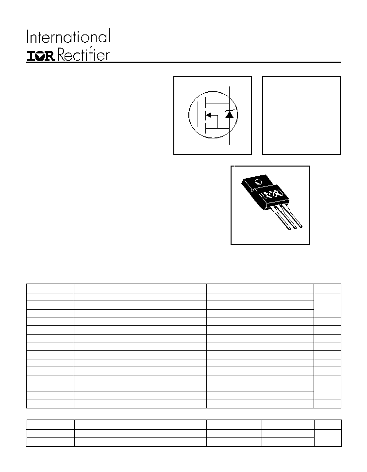
S
D
G
V
DSS
= 55V
R
DS(on)
= 0.012
I
D
= 49A
l
Advanced Process Technology
l
Isolated Package
l
High Voltage Isolation = 2.5KVRMS
l
Sink to Lead Creepage Dist. = 4.8mm
l
Fully Avalanche Rated
TO-220 FULLPAK
Fifth Generation HEXFETs from International Rectifier
utilize advanced processing techniques to achieve
extremely low on-resistance per silicon area. This benefit,
combined with the fast switching speed and ruggedized
device design that HEXFET Power MOSFETs are well
known for, provides the designer with an extremely efficient
and reliable device for use in a wide variety of applications.
The TO-220 Fullpak eliminates the need for additional
insulating hardware in commercial-industrial applications.
The moulding compound used provides a high isolation
capability and a low thermal resistance between the tab
and external heatsink. This isolation is equivalent to using
a 100 micron mica barrier with standard TO-220 product.
The Fullpak is mounted to a heatsink using a single clip or
by a single screw fixing.
8/25/97
Description
Parameter
Max.
Units
I
D
@ T
C
= 25°C
Continuous Drain Current, V
GS
@ 10V
49
I
D
@ T
C
= 100°C
Continuous Drain Current, V
GS
@ 10V
35
A
I
DM
Pulsed Drain Current
290
P
D
@T
C
= 25°C
Power Dissipation
58
W
Linear Derating Factor
0.38
W/°C
V
GS
Gate-to-Source Voltage
± 20
V
E
AS
Single Pulse Avalanche Energy
360
mJ
I
AR
Avalanche Current
43
A
E
AR
Repetitive Avalanche Energy
5.8
mJ
dv/dt
Peak Diode Recovery dv/dt
5.0
V/ns
T
J
Operating Junction and
-55 to + 175
T
STG
Storage Temperature Range
Soldering Temperature, for 10 seconds
300 (1.6mm from case )
°C
Mounting torque, 6-32 or M3 srew
10 lbf·in (1.1N·m)
Absolute Maximum Ratings
Parameter
Typ.
Max.
Units
R
JC
Junction-to-Case
2.6
R
JA
Junction-to-Ambient
65
Thermal Resistance
°C/W
IRFI1010N
Parameter
Min. Typ. Max. Units
Conditions
V
(BR)DSS
Drain-to-Source Breakdown Voltage
55
V
V
GS
= 0V, I
D
= 250µA
V
(BR)DSS
/
T
J
Breakdown Voltage Temp. Coefficient
0.06
V/°C
Reference to 25°C, I
D
= 1mA
R
DS(on)
Static Drain-to-Source On-Resistance
0.012
V
GS
= 10V, I
D
= 26A
V
GS(th)
Gate Threshold Voltage
2.0
4.0
V
V
DS
= V
GS
, I
D
= 250µA
g
fs
Forward Transconductance
30
S
V
DS
= 25V, I
D
= 43A
25
µA
V
DS
= 55V, V
GS
= 0V
250
V
DS
= 44V, V
GS
= 0V, T
J
= 150°C
Gate-to-Source Forward Leakage
100
V
GS
= 20V
Gate-to-Source Reverse Leakage
-100
nA
V
GS
= -20V
Q
g
Total Gate Charge
130
I
D
= 43A
Q
gs
Gate-to-Source Charge
23
nC
V
DS
= 44V
Q
gd
Gate-to-Drain ("Miller") Charge
53
V
GS
= 10V, See Fig. 6 and 13
t
d(on)
Turn-On Delay Time
11
V
DD
= 28V
t
r
Rise Time
66
I
D
= 43A
t
d(off)
Turn-Off Delay Time
40
R
G
= 3.6
t
f
Fall Time
46
R
D
= 0.62
,
See Fig. 10
Between lead,
6mm (0.25in.)
from package
and center of die contact
C
iss
Input Capacitance
2900
V
GS
= 0V
C
oss
Output Capacitance
880
V
DS
= 25V
C
rss
Reverse Transfer Capacitance
330
= 1.0MHz, See Fig. 5
C
Drain to Sink Capacitance
12
= 1.0MHz
nH
Electrical Characteristics @ T
J
= 25°C (unless otherwise specified)
L
D
Internal Drain Inductance
L
S
Internal Source Inductance
S
D
G
I
GSS
ns
4.5
7.5
I
DSS
Drain-to-Source Leakage Current
pF
Notes:
Repetitive rating; pulse width limited by
max. junction temperature. ( See fig. 11 )
V
DD
= 25V, starting T
J
= 25°C, L = 390µH
R
G
= 25
, I
AS
= 43A. (See Figure 12)
t=60s, =60Hz
I
SD
43A, di/dt
260A/µs, V
DD
V
(BR)DSS
,
T
J
175°C
Uses IRF1010N data and test conditions
Pulse width
300µs; duty cycle
2%.
Parameter
Min. Typ. Max. Units
Conditions
I
S
Continuous Source Current
MOSFET symbol
(Body Diode)
showing the
I
SM
Pulsed Source Current
integral reverse
(Body Diode)
p-n junction diode.
V
SD
Diode Forward Voltage
1.3
V
T
J
= 25°C, I
S
= 26A, V
GS
= 0V
t
rr
Reverse Recovery Time
81
120
ns
T
J
= 25°C, I
F
= 43A
Q
rr
Reverse RecoveryCharge
240
370
nC
di/dt = 100A/µs
Source-Drain Ratings and Characteristics
S
D
G
49
290
A
IRFI1010N
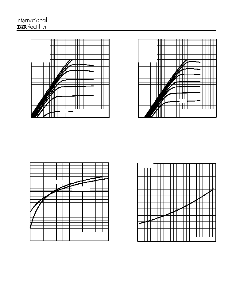
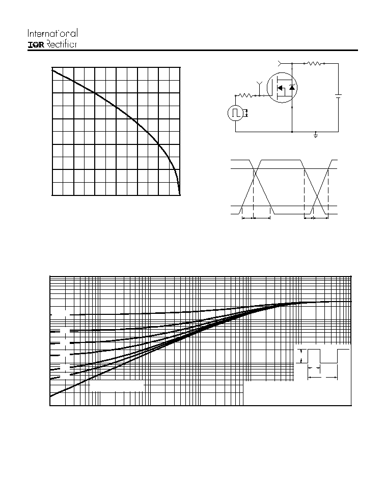
Fig 4. Normalized On-Resistance
Vs. Temperature
Fig 2. Typical Output Characteristics
Fig 1. Typical Output Characteristics
Fig 3. Typical Transfer Characteristics
10
100
1000
0.1
1
10
100
I
,
D
r
a
i
n-
t
o
-
S
ou
r
c
e
C
u
r
r
ent
(
A
)
D
V , D ra in-to-S ou rce V o lta ge (V )
D S
VGS
TOP 15V
10V
8.0V
7.0V
6.0V
5.5V
5.0V
BOTT OM 4.5V
2 0µ s PU LSE W ID TH
T = 2 5°C
C
A
4.5 V
10
100
1000
0.1
1
10
100
4 .5V
I
,
D
r
a
i
n-
t
o
-
S
ou
r
c
e
C
u
r
r
ent
(
A
)
D
V , Dra in -to-So urce V oltag e (V)
D S
VGS
TOP 15V
10V
8.0V
7.0V
6.0V
5.5V
5.0V
BOTT OM 4.5V
20 µs P UL SE W I DTH
T = 17 5°C
C
A
1
1 0
1 0 0
1 0 0 0
4
5
6
7
8
9
1 0
T = 2 5 ° C
J
G S
V , Ga te -to -S o u rce V o lta g e (V )
D
I
, D
r
a
i
n
-
to
-
S
o
u
r
c
e
C
u
r
r
e
n
t
(
A
)
T = 1 7 5 ° C
J
A
V = 2 5 V
2 0 µ s P U L SE W ID TH
DS
0 . 0
0 . 5
1 . 0
1 . 5
2 . 0
2 . 5
3 . 0
- 6 0
- 4 0
- 2 0
0
2 0
4 0
6 0
8 0
1 0 0 1 2 0 1 4 0 1 6 0 1 8 0
J
T , Ju nctio n T emp eratu re (°C)
R
, D
r
a
i
n
-
to
-
S
o
u
r
c
e
O
n
R
e
s
i
s
t
a
n
c
e
D
S
(
on)
(
N
or
m
a
l
i
z
ed)
V = 10 V
G S
A
I = 72 A
D
IRFI1010N
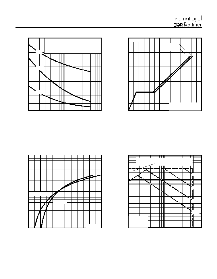
Fig 6. Typical Gate Charge Vs.
Gate-to-Source Voltage
Fig 8. Maximum Safe Operating Area
Fig 5. Typical Capacitance Vs.
Drain-to-Source Voltage
Fig 7. Typical Source-Drain Diode
Forward Voltage
0
1000
2000
3000
4000
5000
1
10
100
C
,
C
a
pac
i
t
anc
e (
p
F
)
D S
V , Drai n-to -So urce V oltag e (V)
A
V = 0 V, f = 1M H z
C = C + C , C SH O RTE D
C = C
C = C + C
G S
is s gs gd ds
rs s gd
o ss ds g d
C
is s
C
o s s
C
rs s
0
4
8
12
16
20
0
20
40
60
80
100
120
140
Q , To tal Ga te Ch arg e (nC )
G
V
,
G
a
te
-
t
o
-
S
o
u
r
c
e
V
o
l
t
a
g
e
(
V
)
GS
A
FO R TES T C IR CU I T
SEE FIG U R E 13
I = 4 3A
V = 4 4V
V = 2 8V
D
DS
DS
1 0
1 0 0
1 0 0 0
0 . 4
0 . 8
1 . 2
1 . 6
2 . 0
2 . 4
2 . 8
T = 25°C
J
V = 0V
G S
V , S o urce-to -Drain Vo lta ge (V )
I
, R
e
v
e
r
s
e
D
r
a
i
n
C
u
r
r
e
n
t
(
A
)
S D
SD
A
T = 17 5°C
J
1
10
100
1000
1
10
100
V , Dra in -to-So urce Vo ltag e (V)
D S
I ,
D
r
a
i
n
C
u
r
r
e
n
t
(
A
)
OPE R ATIO N IN TH IS A RE A LI MI TE D
BY R
D
D S(o n)
10µ s
100µ s
1m s
10m s
A
T = 25 °C
T = 17 5°C
S ing le Pulse
C
J
IRFI1010N
Fig 9. Maximum Drain Current Vs.
Case Temperature
Fig 10a. Switching Time Test Circuit
V
DS
90%
10%
V
GS
t
d(on)
t
r
t
d(off)
t
f
Fig 10b. Switching Time Waveforms
V
DS
Pulse Width
1
µs
Duty Factor
0.1 %
R
D
V
GS
R
G
D.U.T.
10V
+
-
V
DD
Fig 11. Maximum Effective Transient Thermal Impedance, Junction-to-Case
25
50
75
100
125
150
175
0
10
20
30
40
50
T , Case Temperature
( C)
I , Drain Current (A)
°
C
D
0.01
0.1
1
10
0.00001
0.0001
0.001
0.01
0.1
1
10
Notes:
1. Duty factor D =
t / t
2. Peak T = P
x Z
+ T
1
2
J
DM
thJC
C
P
t
t
DM
1
2
t , Rectangular Pulse Duration (sec)
Thermal Response
(Z )
1
thJC
0.01
0.02
0.05
0.10
0.20
D = 0.50
SINGLE PULSE
(THERMAL RESPONSE)