Äîêóìåíòàöèÿ è îïèñàíèÿ www.docs.chipfind.ru
11/04/04
Benefits
l
Improved Gate, Avalanche and Dynamic dV/dt
Ruggedness
l
Fully Characterized Capacitance and Avalanche
SOA
l
Enhanced body diode dV/dt and dI/dt Capability
PD - 96903A
www.irf.com
1
D
2
Pak
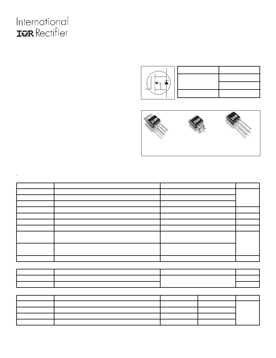
IRFS3507
TO-220AB
IRFB3507
TO-262
IRFSL3507
IRFB3507
IRFS3507
IRFSL3507
HEXFET
®
Power MOSFET
Applications
l
High Efficiency Synchronous Rectification in SMPS
l
Uninterruptible Power Supply
l
High Speed Power Switching
l
Hard Switched and High Frequency Circuits
S
D
G
S
D
G
S
D
G
S
D
G
V
DSS
75V
R
DS(on)
typ.
7.0m:
max.
8.8m:
I
D
97A
Absolute Maximum Ratings
Symbol
Parameter
Units
I
D
@ T
C
= 25°C
Continuous Drain Current, V
GS
@ 10V
A
I
D
@ T
C
= 100°C
Continuous Drain Current, V
GS
@ 10V
I
DM
Pulsed Drain Current
d
P
D
@T
C
= 25°C
Maximum Power Dissipation
W
Linear Derating Factor
W/°C
V
GS
Gate-to-Source Voltage
V
dv/dt
Peak Diode Recovery
f
V/ns
T
J
Operating Junction and
°C
T
STG
Storage Temperature Range
Soldering Temperature, for 10 seconds
(1.6mm from case)
Mounting torque, 6-32 or M3 screw
Avalanche Characteristics
E
AS (Thermally limited)
Single Pulse Avalanche Energy
e
mJ
I
AR
Avalanche Current
c
A
E
AR
Repetitive Avalanche Energy
g
mJ
Thermal Resistance
Symbol
Parameter
Typ.
Max.
Units
R
JC
Junction-to-Case
k
0.77
R
CS
Case-to-Sink, Flat Greased Surface , TO-220
0.50
°C/W
R
JA
Junction-to-Ambient, TO-220
k
62
R
JA
Junction-to-Ambient (PCB Mount) , D
2
Pak
jk
40
280
See Fig. 14, 15, 16a, 16b
190
5.0
-55 to + 175
± 20
1.3
10lb
xin (1.1Nxm)
300
Max.
97
c
69
c
390
IRFB3507/IRFS3507/IRFSL3507
2
www.irf.com
Notes:
Calculated continuous current based on maximum allowable junction
temperature. Package limitation current is 75A.
Repetitive rating; pulse width limited by max. junction
temperature.
Limited by T
Jmax
, starting T
J
= 25°C, L = 0.17mH,
R
G
= 25
, I
AS
= 58A, V
GS
=10V. Part not recommended for use
above this value.
I
SD
58A, di/dt 390A/µs, V
DD
V
(BR)DSS
, T
J
175°C.
Pulse width
400µs; duty cycle 2%.
S
D
G
C
oss
eff. (TR) is a fixed capacitance that gives the same charging time
as C
oss
while V
DS
is rising from 0 to 80% V
DSS
.
C
oss
eff. (ER) is a fixed capacitance that gives the same energy as
C
oss
while V
DS
is rising from 0 to 80% V
DSS
.
When mounted on 1" square PCB (FR-4 or G-10 Material). For recom
mended footprint and soldering techniques refer to application note #AN-994.
R
is measured at T
J
approximately 90°C.
Static @ T
J
= 25°C (unless otherwise specified)
Symbol
Parameter
Min. Typ. Max. Units
V
(BR)DSS
Drain-to-Source Breakdown Voltage
75
V
V
(BR)DSS
/
T
J
Breakdown Voltage Temp. Coefficient
0.070
V/°C
R
DS(on)
Static Drain-to-Source On-Resistance
7.0
8.8
m
V
GS(th)
Gate Threshold Voltage
2.0
4.0
V
I
DSS
Drain-to-Source Leakage Current
20
µA
250
I
GSS
Gate-to-Source Forward Leakage
200
nA
Gate-to-Source Reverse Leakage
-200
R
G
Gate Input Resistance
1.3
f = 1MHz, open drain
Dynamic @ T
J
= 25°C (unless otherwise specified)
Symbol
Parameter
Min. Typ. Max. Units
gfs
Forward Transconductance
86
S
Q
g
Total Gate Charge
88
130
nC
Q
gs
Gate-to-Source Charge
24
Q
gd
Gate-to-Drain ("Miller") Charge
36
t
d(on)
Turn-On Delay Time
20
ns
t
r
Rise Time
81
t
d(off)
Turn-Off Delay Time
52
t
f
Fall Time
49
C
iss
Input Capacitance
3540
pF
C
oss
Output Capacitance
340
C
rss
Reverse Transfer Capacitance
210
C
oss
eff. (ER) Effective Output Capacitance (Energy Related)
460
C
oss
eff. (TR) Effective Output Capacitance (Time Related)h
520
Diode Characteristics
Symbol
Parameter
Min. Typ. Max. Units
I
S
Continuous Source Current
97
c
A
(Body Diode)
I
SM
Pulsed Source Current
390
A
(Body Diode)
d
V
SD
Diode Forward Voltage
1.3
V
t
rr
Reverse Recovery Time
37
56
ns
T
J
= 25°C
V
R
= 64V,
45
68
T
J
= 125°C
I
F
= 58A
Q
rr
Reverse Recovery Charge
32
48
nC T
J
= 25°C
di/dt = 100A/µs
g
51
77
T
J
= 125°C
I
RRM
Reverse Recovery Current
1.7
A
T
J
= 25°C
t
on
Forward Turn-On Time
Intrinsic turn-on time is negligible (turn-on is dominated by LS+LD)
Conditions
V
DS
= 50V, I
D
= 58A
I
D
= 58A
V
GS
= 20V
V
GS
= -20V
MOSFET symbol
showing the
V
DS
= 60V
Conditions
V
GS
= 10V
g
V
GS
= 0V
V
DS
= 50V
= 1.0MHz
V
GS
= 0V, V
DS
= 0V to 60V
i, See Fig.11
V
GS
= 0V, V
DS
= 0V to 60V
h, See Fig. 5
T
J
= 25°C, I
S
= 58A, V
GS
= 0V
g
integral reverse
p-n junction diode.
Conditions
V
GS
= 0V, I
D
= 250µA
Reference to 25°C, I
D
= 1mA
d
V
GS
= 10V, I
D
= 58A
g
V
DS
= V
GS
, I
D
= 100µA
V
DS
= 75V, V
GS
= 0V
V
DS
= 75V, V
GS
= 0V, T
J
= 125°C
I
D
= 58A
R
G
= 5.6
V
GS
= 10V
g
V
DD
= 48V
IRFB3507/IRFS3507/IRFSL3507
www.irf.com
3
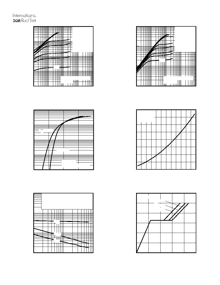
Fig 1. Typical Output Characteristics
Fig 3. Typical Transfer Characteristics
Fig 4. Normalized On-Resistance vs. Temperature
Fig 2. Typical Output Characteristics
Fig 6. Typical Gate Charge vs. Gate-to-Source Voltage
Fig 5. Typical Capacitance vs. Drain-to-Source Voltage
0.1
1
10
100
1000
VDS, Drain-to-Source Voltage (V)
0.1
1
10
100
1000
I D
,
D
r
a
i
n
-
t
o
-
S
o
u
r
c
e
C
u
r
r
e
n
t
(
A
)
VGS
TOP 15V
10V
8.0V
6.0V
5.5V
5.0V
4.8V
BOTTOM
4.5V
60µs PULSE WIDTH
Tj = 25°C
4.5V
0.1
1
10
100
1000
VDS, Drain-to-Source Voltage (V)
1
10
100
1000
I D
,
D
r
a
i
n
-
t
o
-
S
o
u
r
c
e
C
u
r
r
e
n
t
(
A
)
4.5V
60µs PULSE WIDTH
Tj = 175°C
VGS
TOP 15V
10V
8.0V
6.0V
5.5V
5.0V
4.8V
BOTTOM
4.5V
2
4
6
8
10
VGS, Gate-to-Source Voltage (V)
0.1
1
10
100
1000
I D
,
D
r
a
i
n
-
t
o
-
S
o
u
r
c
e
C
u
r
r
e
n
t
(
)
TJ = 25°C
TJ = 175°C
VDS = 25V
60µs PULSE WIDTH
-60 -40 -20 0 20 40 60 80 100120140160180
TJ , Junction Temperature (°C)
0.5
1.0
1.5
2.0
2.5
R
D
S
(
o
n
)
,
D
r
a
i
n
-
t
o
-
S
o
u
r
c
e
O
n
R
e
s
i
s
t
a
n
c
e
(
N
o
r
m
a
l
i
z
e
d
)
ID = 97A
VGS = 10V
1
10
100
VDS, Drain-to-Source Voltage (V)
100
1000
10000
100000
C
,
C
a
p
a
c
i
t
a
n
c
e
(
p
F
)
VGS = 0V, f = 1 MHZ
Ciss = Cgs + Cgd, C ds SHORTED
Crss = Cgd
Coss = Cds + Cgd
Coss
Crss
Ciss
0
20
40
60
80
100
QG Total Gate Charge (nC)
0.0
2.0
4.0
6.0
8.0
10.0
12.0
V
G
S
,
G
a
t
e
-
t
o
-
S
o
u
r
c
e
V
o
l
t
a
g
e
(
V
)
VDS= 60V
VDS= 38V
VDS= 15V
ID= 58A
IRFB3507/IRFS3507/IRFSL3507
4
www.irf.com
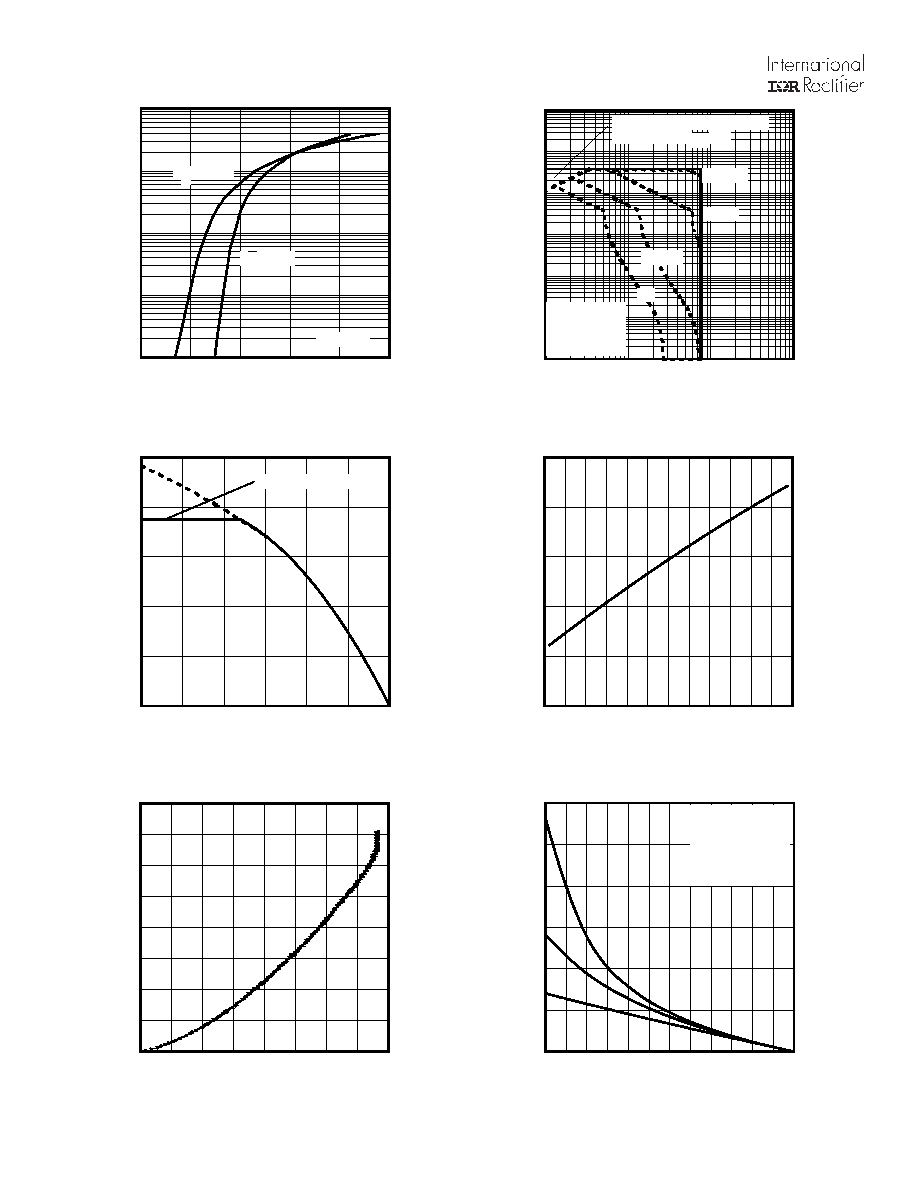
Fig 8. Maximum Safe Operating Area
Fig 10. Drain-to-Source Breakdown Voltage
Fig 7. Typical Source-Drain Diode Forward Voltage
Fig 11. Typical C
OSS
Stored Energy
Fig 9. Maximum Drain Current vs. Case Temperature
Fig 12. Maximum Avalanche Energy vs. DrainCurrent
0.0
0.4
0.8
1.2
1.6
2.0
VSD, Source-to-Drain Voltage (V)
0.1
1
10
100
1000
I S
D
,
R
e
v
e
r
s
e
D
r
a
i
n
C
u
r
r
e
n
t
(
A
)
TJ = 25°C
TJ = 175°C
VGS = 0V
25
50
75
100
125
150
175
TC , Case Temperature (°C)
0
20
40
60
80
100
I D
,
D
r
a
i
n
C
u
r
r
e
n
t
(
A
)
Limited By Package
-60 -40 -20 0 20 40 60 80 100 120 140 160 180
TJ , Temperature ( °C )
70
75
80
85
90
95
V
(
B
R
)
D
S
S
,
D
r
a
i
n
-
t
o
-
S
o
u
r
c
e
B
r
e
a
k
d
o
w
n
V
o
l
t
a
g
e
(
V
)
0
10
20
30
40
50
60
70
80
VDS, Drain-to-Source Voltage (V)
0.0
0.2
0.4
0.6
0.8
1.0
1.2
1.4
1.6
E
n
e
r
g
y
(
µ
J
)
25
50
75
100
125
150
175
Starting TJ , Junction Temperature (°C)
0
200
400
600
800
1000
1200
E
A
S
,
S
i
n
g
l
e
P
u
l
s
e
A
v
a
l
a
n
c
h
e
E
n
e
r
g
y
(
m
J
)
ID
TOP 8.9A
12A
BOTTOM 58A
1
10
100
1000
VDS, Drain-to-Source Voltage (V)
0.01
0.1
1
10
100
1000
10000
I D
,
D
r
a
i
n
-
t
o
-
S
o
u
r
c
e
C
u
r
r
e
n
t
(
A
)
OPERATION IN THIS AREA
LIMITED BY RDS(on)
Tc = 25°C
Tj = 175°C
Single Pulse
100µsec
1msec
10msec
DC
IRFB3507/IRFS3507/IRFSL3507
www.irf.com
5
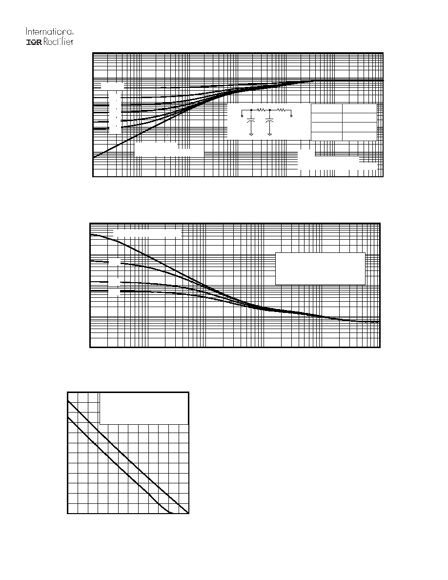
Fig 13. Maximum Effective Transient Thermal Impedance, Junction-to-Case
Fig 14. Typical Avalanche Current vs.Pulsewidth
Fig 15. Maximum Avalanche Energy vs. Temperature
Notes on Repetitive Avalanche Curves , Figures 14, 15:
(For further info, see AN-1005 at www.irf.com)
1. Avalanche failures assumption:
Purely a thermal phenomenon and failure occurs at a temperature far in
excess of T
jmax
. This is validated for every part type.
2. Safe operation in Avalanche is allowed as long asT
jmax
is not exceeded.
3. Equation below based on circuit and waveforms shown in Figures 16a, 16b.
4. P
D (ave)
= Average power dissipation per single avalanche pulse.
5. BV = Rated breakdown voltage (1.3 factor accounts for voltage increase
during avalanche).
6. I
av
= Allowable avalanche current.
7.
T
=
Allowable rise in junction temperature, not to exceed
T
jmax
(assumed as
25°C in Figure 14, 15).
t
av =
Average time in avalanche.
D = Duty cycle in avalanche = t
av
·f
Z
thJC
(D, t
av
) = Transient thermal resistance, see Figures 13)
P
D (ave)
= 1/2 ( 1.3·BV·I
av
) =
DT/ Z
thJC
I
av
=
2
DT/ [1.3·BV·Z
th
]
E
AS (AR)
= P
D (ave)
·t
av
1E-006
1E-005
0.0001
0.001
0.01
0.1
1
t1 , Rectangular Pulse Duration (sec)
0.0001
0.001
0.01
0.1
1
10
T
h
e
r
m
a
l
R
e
s
p
o
n
s
e
(
Z
t
h
J
C
)
0.20
0.10
D = 0.50
0.02
0.01
0.05
SINGLE PULSE
( THERMAL RESPONSE )
Notes:
1. Duty Factor D = t1/t2
2. Peak Tj = P dm x Zthjc + Tc
Ri (°C/W)
i (sec)
0.2963 0.000504
0.4738 0.013890
J
J
1
1
2
2
R
1
R
1
R
2
R
2
C
Ci i
/Ri
Ci=
i/Ri
1.0E-06
1.0E-05
1.0E-04
1.0E-03
1.0E-02
1.0E-01
tav (sec)
0.1
1
10
100
1000
A
v
a
l
a
n
c
h
e
C
u
r
r
e
n
t
(
A
)
0.05
Duty Cycle = Single Pulse
0.10
Allowed avalanche Current vs
avalanche pulsewidth, tav
assuming
Tj = 25°C due to
avalanche losses
0.01
25
50
75
100
125
150
175
Starting TJ , Junction Temperature (°C)
0
50
100
150
200
250
300
E
A
R
,
A
v
a
l
a
n
c
h
e
E
n
e
r
g
y
(
m
J
)
TOP Single Pulse
BOTTOM 1% Duty Cycle
ID = 58A