IRF9Z24N
HEXFET
®
Power MOSFET
PD -9.1484B
Fifth Generation HEXFETs from International Rectifier
utilize advanced processing techniques to achieve
extremely low on-resistance per silicon area. This
benefit, combined with the fast switching speed and
ruggedized device design that HEXFET Power
MOSFETs are well known for, provides the designer
with an extremely efficient and reliable device for use
in a wide variety of applications.
The TO-220 package is universally preferred for all
commercial-industrial applications at power dissipation
levels to approximately 50 watts. The low thermal
resistance and low package cost of the TO-220
contribute to its wide acceptance throughout the
industry.
Parameter
Max.
Units
I
D
@ T
C
= 25°C
Continuous Drain Current, V
GS
@ -10V
-12
I
D
@ T
C
= 100°C
Continuous Drain Current, V
GS
@ -10V
-8.5
A
I
DM
Pulsed Drain Current
-48
P
D
@T
C
= 25°C
Power Dissipation
45
W
Linear Derating Factor
0.30
W/°C
V
GS
Gate-to-Source Voltage
± 20
V
E
AS
Single Pulse Avalanche Energy
96
mJ
I
AR
Avalanche Current
-7.2
A
E
AR
Repetitive Avalanche Energy
4.5
mJ
dv/dt
Peak Diode Recovery dv/dt
-5.0
V/ns
T
J
Operating Junction and
-55 to + 175
T
STG
Storage Temperature Range
Soldering Temperature, for 10 seconds
300 (1.6mm from case )
°C
Mounting torque, 6-32 or M3 screw
10 lbf·in (1.1N·m)
Absolute Maximum Ratings
Parameter
Typ.
Max.
Units
R
JC
Junction-to-Case
3.3
R
CS
Case-to-Sink, Flat, Greased Surface
0.50
°C/W
R
JA
Junction-to-Ambient
62
Thermal Resistance
V
DSS
= -55V
R
DS(on)
= 0.175
I
D
= -12A
TO-220AB
l
Advanced Process Technology
l
Dynamic dv/dt Rating
l
175°C Operating Temperature
l
Fast Switching
l
P-Channel
l
Fully Avalanche Rated
Description
8/27/97
S
D
G
IRF9Z24N
Parameter
Min. Typ. Max. Units
Conditions
I
S
Continuous Source Current
MOSFET symbol
(Body Diode)
showing the
I
SM
Pulsed Source Current
integral reverse
(Body Diode)
p-n junction diode.
V
SD
Diode Forward Voltage
-1.6
V
T
J
= 25°C, I
S
= -7.2A, V
GS
= 0V
t
rr
Reverse Recovery Time
47
71
ns
T
J
= 25°C, I
F
= -7.2A
Q
rr
Reverse RecoveryCharge
84
130
µC
di/dt = -100A/µs
t
on
Forward Turn-On Time
Intrinsic turn-on time is negligible (turn-on is dominated by L
S
+L
D
)
Parameter
Min. Typ. Max. Units
Conditions
V
(BR)DSS
Drain-to-Source Breakdown Voltage
-55
V
V
GS
= 0V, I
D
= -250µA
V
(BR)DSS
/
T
J
Breakdown Voltage Temp. Coefficient
-0.05
V/°C
Reference to 25°C, I
D
= -1mA
R
DS(on)
Static Drain-to-Source On-Resistance
0.175
V
GS
= -10V, I
D
= -7.2A
V
GS(th)
Gate Threshold Voltage
-2.0
-4.0
V
V
DS
= V
GS
, I
D
= -250µA
g
fs
Forward Transconductance
2.5
S
V
DS
= -25V, I
D
= -7.2A
-25
µA
V
DS
= -55V, V
GS
= 0V
-250
V
DS
= -44V, V
GS
= 0V, T
J
= 150°C
Gate-to-Source Forward Leakage
100
V
GS
= 20V
Gate-to-Source Reverse Leakage
-100
nA
V
GS
= -20V
Q
g
Total Gate Charge
19
I
D
= -7.2A
Q
gs
Gate-to-Source Charge
5.1
nC
V
DS
= -44V
Q
gd
Gate-to-Drain ("Miller") Charge
10
V
GS
= -10V, See Fig. 6 and 13
t
d(on)
Turn-On Delay Time
13
V
DD
= -28V
t
r
Rise Time
55
I
D
= -7.2A
t
d(off)
Turn-Off Delay Time
23
R
G
= 24
t
f
Fall Time
37
R
D
= 3.7
,
See Fig. 10
Between lead,
6mm (0.25in.)
from package
and center of die contact
C
iss
Input Capacitance
350
V
GS
= 0V
C
oss
Output Capacitance
170
pF
V
DS
= -25V
C
rss
Reverse Transfer Capacitance
92
= 1.0MHz, See Fig. 5
nH
Electrical Characteristics @ T
J
= 25°C (unless otherwise specified)
L
D
Internal Drain Inductance
L
S
Internal Source Inductance
I
GSS
ns
4.5
7.5
I
DSS
Drain-to-Source Leakage Current
Repetitive rating; pulse width limited by
max. junction temperature. ( See fig. 11 )
I
SD
-7.2A, di/dt
-280A/µs, V
DD
V
(BR)DSS
,
T
J
175°C
Notes:
Starting T
J
= 25°C, L = 3.7mH
R
G
= 25
, I
AS
= -7.2A. (See Figure 12)
Pulse width
300µs; duty cycle
2%.
S
D
G
Source-Drain Ratings and Characteristics
A
S
D
G
-12
-48

IRF9Z24N
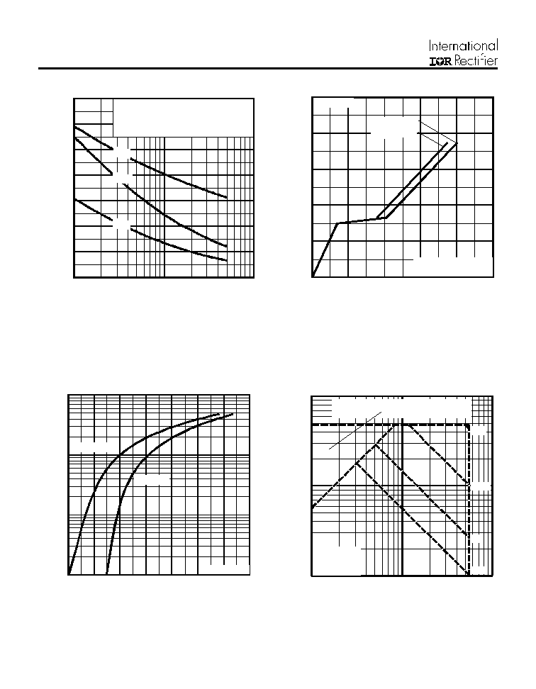
Fig 4. Normalized On-Resistance
Vs. Temperature
Fig 2. Typical Output Characteristics,
Fig 1. Typical Output Characteristics,
Fig 3. Typical Transfer Characteristics
1
1 0
1 0 0
0 . 1
1
1 0
1 0 0
D
D S
2 0µ s PU LS E W ID TH
T = 2 5°C
A
-
I
,
D
r
ai
n-
t
o
-
S
our
c
e
C
u
r
r
ent
(
A
)
-V , Drain -to -So urce Vo ltag e (V)
VGS
TOP - 15V
- 10V
- 8.0V
- 7.0V
- 6.0V
- 5.5V
- 5.0V
BOTT OM - 4. 5V
-4.5 V
c
1
10
100
0.1
1
10
100
D
D S
A
-
I
,
D
r
ai
n-
t
o
-
S
o
u
r
c
e
C
u
r
r
en
t
(
A
)
-V , Dra in -to-So urce V oltag e (V )
VGS
TOP - 15V
- 10V
- 8.0V
- 7.0V
- 6.0V
- 5.5V
- 5.0V
BOTT OM - 4. 5V
-4.5 V
20 µ s PU LSE W ID TH
T = 1 75°C
C
1
1 0
1 0 0
4
5
6
7
8
9
1 0
T = 2 5 °C
J
G S
D
A
-
I
,
D
r
a
i
n
-
t
o
-S
o
u
rc
e
C
u
rre
n
t
(A
)
-V , Ga te -to -S o u rce V o ltag e (V )
V = -2 5 V
2 0 µ s P U L S E W ID T H
DS
T = 1 7 5 °C
J
0 . 0
0 . 5
1 . 0
1 . 5
2 . 0
- 6 0
- 4 0
- 2 0
0
2 0
4 0
6 0
8 0
1 0 0 1 2 0 1 4 0 1 6 0 1 8 0
J
T , Ju nctio n T emp eratu re (°C)
R
,
D
r
a
i
n
-
to
-
S
o
u
r
c
e
O
n
R
e
s
i
s
t
a
n
c
e
D
S
(
on)
(
N
o
r
m
a
l
i
z
ed)
A
V = -10 V
G S
I = -12 A
D
J
J
IRF9Z24N
Fig 8. Maximum Safe Operating Area
Fig 6. Typical Gate Charge Vs.
Gate-to-Source Voltage
Fig 5. Typical Capacitance Vs.
Drain-to-Source Voltage
Fig 7. Typical Source-Drain Diode
Forward Voltage
0
4
8
12
16
20
0
5
10
15
20
25
G
GS
A
-
V
,
G
a
t
e
-
t
o
-
S
our
c
e
V
o
l
t
age (
V
)
Q , Tota l Gate Ch arge (n C)
FO R TEST C IR C U IT
SEE F IGU R E 1 3
I = -7.2 A
V = -4 4V
V = -2 8V
D
DS
DS
0 . 1
1
1 0
1 0 0
0 . 4
0 . 6
0 . 8
1 . 0
1 . 2
1 . 4
1 . 6
1 . 8
T = 25 °C
T = 1 50°C
J
J
V = 0 V
G S
S D
SD
A
-I
,
R
e
v
e
rs
e
D
r
a
i
n
C
u
rre
n
t
(A
)
-V , S ou rce -to -Drain V olta ge (V )
1
10
100
1
10
100
O PER ATIO N IN TH IS AR EA LIM ITED
BY R
D S(o n)
10m s
A
-
I
, D
r
a
i
n
C
u
r
r
e
n
t (
A
)
-V , Dra in-to-So urce V olta ge (V )
D S
D
1 0µs
100µ s
1m s
T = 2 5°C
T = 1 75°C
Sin gle Pu ls e
C
J
0
100
200
300
400
500
600
700
1
10
100
C
,
C
a
pac
i
t
anc
e (
p
F
)
D S
V , Drai n-to -So urce V oltag e (V)
A
V = 0V , f = 1MH z
C = C + C , C SH OR TED
C = C
C = C + C
G S
is s gs g d ds
rs s g d
os s ds gd
C
is s
C
o s s
C
rs s

IRF9Z24N
Fig 10a. Switching Time Test Circuit
Fig 10b. Switching Time Waveforms
Fig 11. Maximum Effective Transient Thermal Impedance, Junction-to-Case
Fig 9. Maximum Drain Current Vs.
Case Temperature
V
DS
-10V
Pulse Width
1
µs
Duty Factor
0.1 %
R
D
V
GS
V
DD
R
G
D.U.T.
+
-
V
DS
90%
10%
V
GS
t
d(on)
t
r
t
d(off)
t
f
0
3
6
9
1 2
2 5
5 0
7 5
1 0 0
1 2 5
1 5 0
1 7 5
C
T , C ase T emp era ture (°C)
A
-
I
,
D
r
ai
n C
u
r
r
ent
(
A
m
p
s
)
D
0 . 0 1
0 . 1
1
1 0
0 . 0 0 0 0 1
0 . 0 0 0 1
0 . 0 0 1
0 . 0 1
0 . 1
1
t , R ectan gula r P u lse D uratio n (sec)
1
th
J
C
D = 0 .5 0
0 .0 1
0 .0 2
0 .0 5
0 .1 0
0 .2 0
S IN G LE P U L S E
(T H E R M A L R E S P O N S E )
A
T
her
m
a
l
R
e
s
pons
e
(
Z
)
P
t
2
1
t
DM
N otes :
1. D uty fac tor D = t / t
2. P ea k T = P x Z + T
1
2
J
D M
th JC
C