N-Channel
P-Channel
Drain-Source Voltage
V
DS
30
Gate-Source Voltage
V
GS
± 20
T
A
= 25°C
3.5
-2.3
T
A
= 70°C
2.8
-1.8
Pulsed Drain Current
I
DM
16
-10
Continuous Source Current (Diode Conduction)
I
S
1.7
-1.3
T
A
= 25°C
2.0
T
A
= 70°C
1.3
Single Pulse Avalanche Energy
E
AS
44
57
mJ
Avalanche Current
I
AR
2.0
-1.3
A
Repetitive Avalanche Energy
E
AR
0.25
mJ
Peak Diode Recovery dv/dt
dv/dt
5.0
-5.0
V/ ns
Junction and Storage Temperature Range
T
J,
T
STG
-55 to + 150 °C
PRELIMINARY
HEXFET
®
Power MOSFET
PD - 9.1561A
Fifth Generation HEXFETs from International Rectifier
utilize advanced processing techniques to achieve
extremely low on-resistance per silicon area. This
benefit, combined with the fast switching speed and
ruggedized device design that HEXFET Power
MOSFETs are well known for, provides the designer
with an extremely efficient and reliable device for use
in a wide variety of applications.
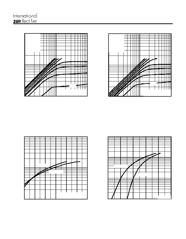
The SO-8 has been modified through a customized
leadframe for enhanced thermal characteristics and
multiple-die capability making it ideal in a variety of
power applications. With these improvements, multiple
devices can be used in an application with dramatically
reduced board space. The package is designed for
vapor phase, infra red, or wave soldering techniques.
8/25/97
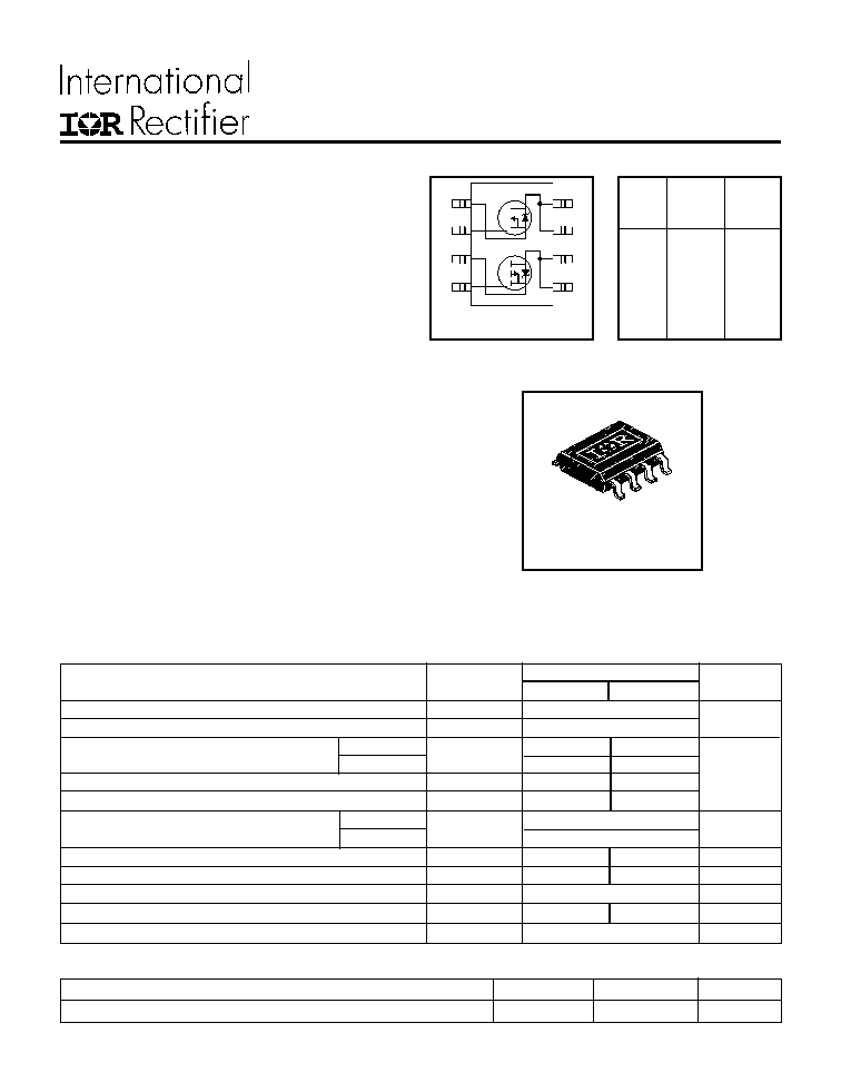
S O -8
l
Generation V Technology
l
Ultra Low On-Resistance
l
Dual N and P Channel MOSFET
l
Surface Mount
l
Very Low Gate Charge and
Switching Losses
l
Fully Avalanche Rated
IRF9952
Description
Thermal Resistance Ratings
Parameter
Symbol
Limit
Units
Maximum Junction-to-Ambient
R
JA
62.5
°C/W
Continuous Drain Current
Maximum Power Dissipation
A
I
D
P
D
V
W
Symbol Maximum
Units
D1
N -C H A N N E L M O S F E T
P -C H A N N E L M O S F E T
D 1
D2
D 2
G 1
S 2
G 2
S 1
T o p V iew
8
1
2
3
4
5
6
7
N-Ch P-Ch
V
DSS
30V
-30V
R
DS(on)
0.10
0.25
Recommended upgrade: IRF7309 or IRF7319
Lower profile/smaller equivalent: IRF7509
IRF9952
Surface mounted on FR-4 board, t
10sec.
Parameter
Min. Typ. Max. Units
Conditions
N-Ch 30
--
--
V
GS
= 0V, I
D
= 250µA
P-Ch -30
--
--
V
GS
= 0V, I
D
= -250µA
N-Ch
-- 0.015
--
Reference to 25°C, I
D
= 1mA
P-Ch
-- 0.015
--
Reference to 25°C, I
D
= -1mA
--
0.08 0.10
V
GS
= 10V, I
D
= 2.2A
--
0.12 0.15
V
GS
= 4.5V, I
D
= 1.0A
-- 0.165 0.250
V
GS
= -10V, I
D
= -1.0A
-- 0.290 0.400
V
GS
= -4.5V, I
D
= -0.50A
N-Ch 1.0
--
--
V
DS
= V
GS
, I
D
= 250µA
P-Ch -1.0
--
--
V
DS
= V
GS
, I
D
= -250µA
N-Ch
--
12
--
V
DS
= 15V, I
D
= 3.5A
P-Ch
--
2.4
--
V
DS
= -15V, I
D
= -2.3A
N-Ch
--
--
2.0
V
DS
= 24V, V
GS
= 0V
P-Ch
--
--
-2.0
V
DS
= -24V, V
GS
= 0V
N-Ch
--
--
25
V
DS
= 24V, V
GS
= 0V, T
J
= 125°C
P-Ch
--
--
-25
V
DS
= -24V, V
GS
= 0V, T
J
= 125°C
I
GSS
Gate-to-Source Forward Leakage
N-P
--
±100
V
GS
= ±20V
N-Ch
--
6.9
14
P-Ch
--
6.1
12
N-Ch
--
1.0
2.0
P-Ch
--
1.7
3.4
N-Ch
--
1.8
3.5
P-Ch
--
1.1
2.2
N-Ch
--
6.2
12
P-Ch
--
9.7
19
N-Ch
--
8.8
18
P-Ch
--
14
28
N-Ch
--
13
26
P-Ch
--
20
40
N-Ch
--
3.0
6.0
P-Ch
--
6.9
14
N-Ch
--
190
--
P-Ch
--
190
--
N-Ch
--
120
--
pF
P-Ch
--
110
--
N-Ch
--
61
--
P-Ch
--
54
--
V
(BR)DSS
Drain-to-Source Breakdown Voltage
V
(BR)DSS
/
T
J
Breakdown Voltage Temp. Coefficient
R
DS(ON)
Static Drain-to-Source On-Resistance
V
GS(th)
Gate Threshold Voltage
g
fs
Forward Transconductance
I
DSS
Drain-to-Source Leakage Current
Q
g
Total Gate Charge
Q
gs
Gate-to-Source Charge
Q
gd
Gate-to-Drain ("Miller") Charge
t
d(on)
Turn-On Delay Time
t
r
Rise Time
t
d(off)
Turn-Off Delay Time
t
f
Fall Time
C
iss
Input Capacitance
C
oss
Output Capacitance
C
rss
Reverse Transfer Capacitance
Electrical Characteristics @ T
J
= 25°C (unless otherwise specified)
V
V/°C
V
S
µA
nC
ns
N-Channel
I
D
= 1.8A, V
DS
= 10V, V
GS
= 10V
P-Channel
I
D
= -2.3A, V
DS
= -10V, V
GS
= -10V
N-Channel
V
DD
= 10V, I
D
= 1.0A, R
G
= 6.0
,
R
D
= 10
P-Channel
V
DD
= -10V, I
D
= -1.0A, R
G
= 6.0
,
R
D
= 10
N-Channel
V
GS
= 0V, V
DS
= 15V, = 1.0MHz
P-Channel
V
GS
= 0V, V
DS
= -15V, = 1.0MHz
N-Ch
P-Ch
Parameter
Min. Typ. Max. Units
Conditions
N-Ch
--
--
1.7
P-Ch
--
--
-1.3
N-Ch
--
--
16
P-Ch
--
--
16
N-Ch
--
0.82
1.2
T
J
= 25°C, I
S
= 1.25A, V
GS
= 0V
P-Ch
--
-0.82 -1.2
T
J
= 25°C, I
S
= -1.25A, V
GS
= 0V
N-Ch
--
27
53
P-Ch
--
27
54
N-Ch
--
28
57
P-Ch
--
31
62
Source-Drain Ratings and Characteristics
I
S
Continuous Source Current (Body Diode)
I
SM
Pulsed Source Current (Body Diode)
V
SD
Diode Forward Voltage
t
rr
Reverse Recovery Time
Q
rr
Reverse Recovery Charge
A
V
ns
nC
N-Channel
T
J
= 25°C, I
F
=1.25A, di/dt = 100A/µs
P-Channel
T
J
= 25°C, I
F
= -1.25A, di/dt = 100A/µs
N-Channel I
SD
2.0A, di/dt
100A/µs, V
DD
V
(BR)DSS
, T
J
150°C
P-Channel I
SD
-1.3A, di/dt
84A/µs, V
DD
V
(BR)DSS
, T
J
150°C
Repetitive rating; pulse width limited by
max. junction temperature. ( See fig. 23 )
Notes:
Pulse width
300µs; duty cycle
2%.
N-Channel Starting T
J
= 25°C, L = 22mH R
G
= 25
, I
AS
= 2.0A. (See Figure 12)
P-Channel Starting T
J
= 25°C, L = 67mH R
G
= 25
, I
AS
= -1.3A.
nA
IRF9952
Fig 3. Typical Transfer Characteristics
Fig 2. Typical Output Characteristics
Fig 1. Typical Output Characteristics
Fig 4. Typical Source-Drain Diode
Forward Voltage
N-Channel
1
1 0
1 0 0
0 . 1
1
1 0
20 µs P U LSE W I DTH
T = 25 °C
A
J
D S
V , D ra in-to-S ou rce V o lta ge (V )
3. 0V
VGS
TOP 15V
10V
7.0V
5.5V
4.5V
4.0V
3.5V
BOTT OM 3.0V
DI
,
D
r
ai
n
-
t
o
-
S
our
c
e
C
u
r
r
ent
(
A
)
1
1 0
1 0 0
0 . 1
1
1 0
A
D S
V , D rain-to -S ou rce Vo lta ge (V)
D
I
,
D
r
ai
n
-
t
o
-
S
our
c
e
C
u
r
r
ent
(
A
)
20 µs P U LSE W I DTH
T = 15 0°C
J
3 .0V
VGS
TOP 15V
10V
7.0V
5.5V
4.5V
4.0V
3.5V
BOTT OM 3.0V
0 . 1
1
1 0
1 0 0
0 . 4
0 . 6
0 . 8
1 . 0
1 . 2
1 . 4
T = 2 5°C
T = 1 50 °C
J
J
V = 0 V
G S
V , So urce-to -D rain V olta ge (V )
I
, R
e
v
e
r
s
e
D
r
a
i
n
C
u
r
r
e
n
t
(
A
)
S D
SD
A
1
1 0
1 0 0
3 . 0
3 . 5
4 . 0
4 . 5
5 . 0
5 . 5
6 . 0
T = 2 5 °C
T = 1 5 0 °C
J
J
G S
V , Ga te -to -S o u rce V o lta g e (V )
D
I
, D
r
a
i
n
-
to
-
S
o
u
r
c
e
C
u
r
r
e
n
t
(
A
)
A
V = 1 0 V
2 0 µ s PU L SE W ID TH
D S
IRF9952
Fig 5. Normalized On-Resistance
Vs. Temperature
Fig 8. Maximum Avalanche Energy
Vs. Drain Current
Fig 6. Typical On-Resistance Vs. Drain
Current
Fig 7. Typical On-Resistance Vs. Gate
Voltage
N-Channel
-60 -40 -20
0
20
40
60
80 100 120 140 160
0.0
0.5
1.0
1.5
2.0
T , Junction Temperature ( C)
R , Drain-to-Source On Resistance
(Normalized)
J
DS(on)
°
V
=
I =
GS
D
10V
2.2A
0 . 0 0
0 . 0 2
0 . 0 4
0 . 0 6
0 . 0 8
0 . 1 0
0 . 1 2
0 . 1 4
0 . 1 6
0
3
6
9
1 2
1 5
A
I = 3 .5A
D
G S
V , G a te -to -S o urce V oltage (V)
R
DS
(on) , Drain-to-Source On Resistance (
)
0
20
40
60
80
100
25
50
75
100
125
150
J
E , Single Pulse Avalanche Energy (mJ)
AS
A
Starting T , Junction Temperature (°C)
I
TOP 0.89A
1.6A
BOTTOM 2.0A
D
0 . 0 4
0 . 0 6
0 . 0 8
0 . 1 0
0 . 1 2
0
2
4
6
8
1 0
1 2
A
I , D ra in C ur re nt (A)
D
V = 10V
G S
V = 4. 5V
G S
R
DS
(on) , Drain-to-Source On Resistance (
)
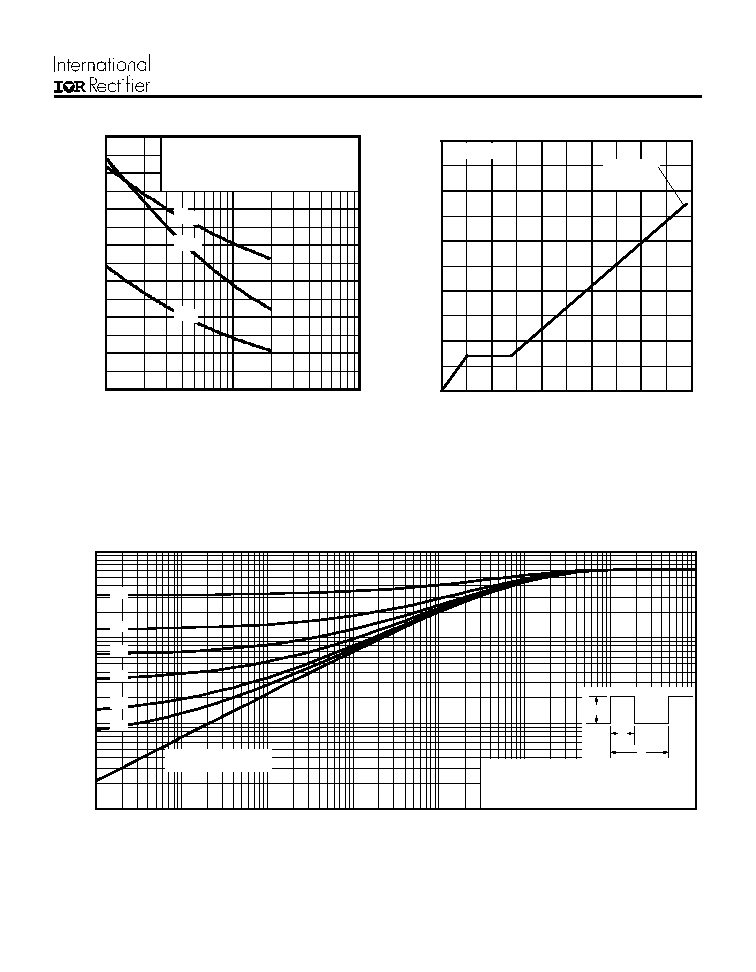
IRF9952
Fig 11. Maximum Effective Transient Thermal Impedance, Junction-to-Ambient
Fig 10. Typical Gate Charge Vs.
Gate-to-Source Voltage
Fig 9. Typical Capacitance Vs.
Drain-to-Source Voltage
N-Channel
0
50
100
150
200
250
300
350
1
10
100
C
,
C
a
pac
i
t
anc
e (
p
F
)
D S
V , Drai n-to -So urce V oltag e (V)
A
V = 0 V, f = 1M H z
C = C + C , C SH O RTE D
C = C
C = C + C
G S
is s gs gd ds
rs s gd
o ss ds g d
C
is s
C
o s s
C
rs s
0
2
4
6
8
10
0
4
8
12
16
20
Q , Total Gate Charge (nC)
V , Gate-to-Source Voltage (V)
G
GS
I =
D
1.8A
V
= 10V
DS
0.1
1
10
100
0.00001
0.0001
0.001
0.01
0.1
1
10
100
Notes:
1. Duty factor D =
t / t
2. Peak T
= P
x Z
+ T
1
2
J
DM
thJA
A
P
t
t
DM
1
2
t , Rectangular Pulse Duration (sec)
Thermal Response
(Z )
1
thJA
0.01
0.02
0.05
0.10
0.20
0.50
SINGLE PULSE
(THERMAL RESPONSE)