IRF8010S_L.pmd
Notes
through
are on page 8
www.irf.com
1
01/28/03
IRF8010S
IRF8010L
SMPS MOSFET
HEXFET
®
Power MOSFET
V
DSS
R
DS(on)
max
I
D
100V
15m
80A
PD - 94573
Applications
l
High frequency DC-DC converters
l
UPS and Motor Control
Benefits
l
Low Gate-to-Drain Charge to Reduce
Switching Losses
l
Fully Characterized Capacitance Including
Effective C
OSS
to Simplify Design, (See
App. Note AN1001)
l
Fully Characterized Avalanche Voltage
and Current
l
Typical R
DS(on)
= 12m
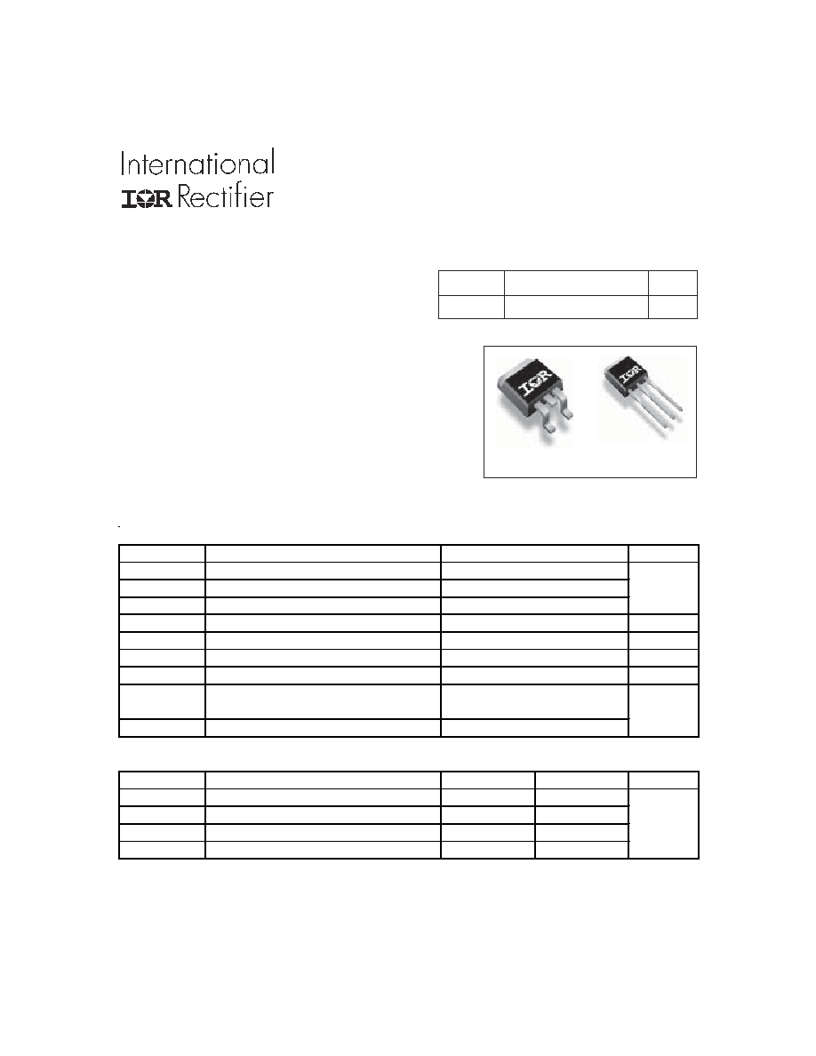
D
2
Pak
IRF8010S
TO-262
IRF8010L
Absolute Maximum Ratings
Parameter
Units
I
D
@ T
C
= 25°C
Continuous Drain Current, V
GS
@ 10V
I
D
@ T
C
= 100°C Continuous Drain Current, V
GS
@ 10V
A
I
DM
Pulsed Drain Current
c
P
D
@T
C
= 25°C Power Dissipation
W
Linear Derating Factor
W/°C
V
GS
Gate-to-Source Voltage
V
dv/dt
Peak Diode Recovery dv/dt
e
V/ns
T
J
Operating Junction and
T
STG
Storage Temperature Range
°C
Soldering Temperature, for 10 seconds
Thermal Resistance
Parameter
Typ.
Max.
Units
R
JC
Junction-to-Case
0.57
R
JC
Junction-to-Case (end of life)
g
0.80
°C/W
R
CS
Case-to-Sink, Flat, Greased Surface
0.50
R
JA
Junction-to-Ambient (PCB Mount, steady state)
j
40
16
-55 to + 175
300 (1.6mm from case )
Max.
80
i
57
320
260
1.8
± 20
IRF8010S/IRF8010L
2
www.irf.com
S
D
G
Static @ T
J
= 25°C (unless otherwise specified)
Parameter
Min. Typ. Max. Units
V
(BR)DSS
Drain-to-Source Breakdown Voltage
100
V
V
(BR)DSS
/
T
J
Breakdown Voltage Temp. Coefficient
0.11
V/°C
R
DS(on)
Static Drain-to-Source On-Resistance
12
15
m
V
GS(th)
Gate Threshold Voltage
2.0
4.0
V
I
DSS
Drain-to-Source Leakage Current
20
µA
250
I
GSS
Gate-to-Source Forward Leakage
200
nA
Gate-to-Source Reverse Leakage
-200
Dynamic @ T
J
= 25°C (unless otherwise specified)
Parameter
Min. Typ. Max. Units
gfs
Forward Transconductance
82
V
Q
g
Total Gate Charge
81
120
Q
gs
Gate-to-Source Charge
22
nC
Q
gd
Gate-to-Drain ("Miller") Charge
26
t
d(on)
Turn-On Delay Time
15
t
r
Rise Time
130
t
d(off)
Turn-Off Delay Time
61
ns
t
f
Fall Time
120
C
iss
Input Capacitance
3830
C
oss
Output Capacitance
480
C
rss
Reverse Transfer Capacitance
59
pF
C
oss
Output Capacitance
3830
C
oss
Output Capacitance
280
C
oss
eff.
Effective Output Capacitance
530
Avalanche Characteristics
Parameter
Units
E
AS
Single Pulse Avalanche Energy
di
mJ
I
AR
Avalanche Current
Ã
A
E
AR
Repetitive Avalanche Energy
mJ
Diode Characteristics
Parameter
Min. Typ. Max. Units
I
S
Continuous Source Current
80
(Body Diode)
A
I
SM
Pulsed Source Current
320
(Body Diode)
Ãi
V
SD
Diode Forward Voltage
1.3
V
t
rr
Reverse Recovery Time
99
150
ns
Q
rr
Reverse RecoveryCharge
460
700
nC
t
on
Forward Turn-On Time
Intrinsic turn-on time is negligible (turn-on is dominated by LS+LD)
V
GS
= 20V
V
GS
= -20V
Max.
V
GS
= 0V, V
DS
= 1.0V, = 1.0MHz
V
GS
= 0V, V
DS
= 80V, = 1.0MHz
V
GS
= 0V, V
DS
= 0V to 80V
e
V
GS
= 10V
f
V
DD
= 50V
I
D
= 80A
R
G
= 39
T
J
= 25°C, I
S
= 80A, V
GS
= 0V
f
T
J
= 150°C, I
F
= 80A, V
DD
= 50V
di/dt = 100A/µs
f
Conditions
V
GS
= 0V, I
D
= 250µA
Reference to 25°C, I
D
= 1mA
V
GS
= 10V, I
D
= 45A
f
V
DS
= V
GS
, I
D
= 250µA
V
DS
= 100V, V
GS
= 0V
V
DS
= 100V, V
GS
= 0V, T
J
= 125°C
MOSFET symbol
showing the
integral reverse
p-n junction diode.
Conditions
26
V
GS
= 10V
f
V
GS
= 0V
V
DS
= 25V
= 1.0MHz
310
45
Conditions
V
DS
= 25V, I
D
= 45A
I
D
= 80A
V
DS
= 80V
Typ.
IRF8010S/IRF8010L
www.irf.com
3
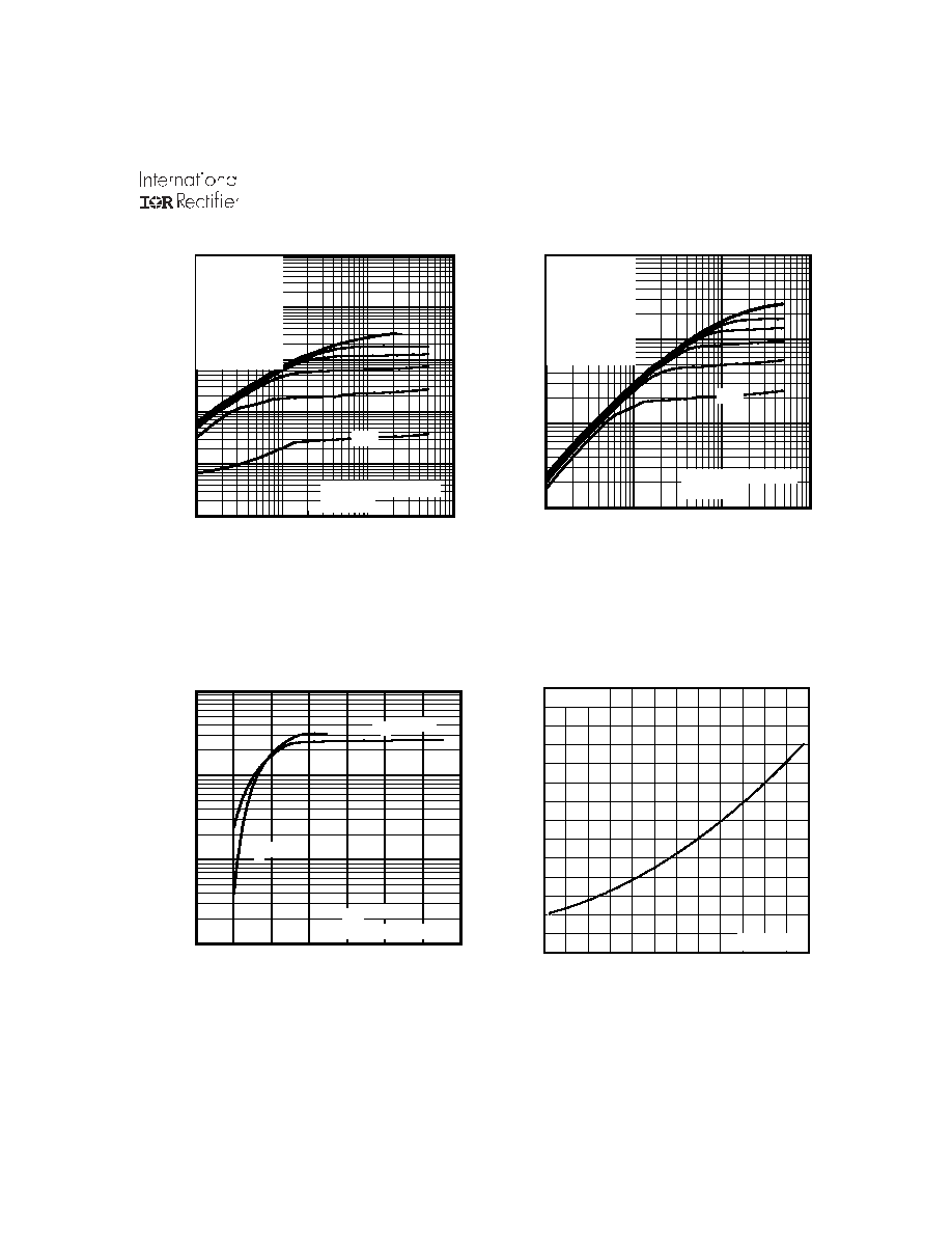
Fig 4. Normalized On-Resistance
Vs. Temperature
Fig 2. Typical Output Characteristics
Fig 1. Typical Output Characteristics
Fig 3. Typical Transfer Characteristics
-60
-40
-20
0
20
40
60
80
100 120 140 160 180
0.0
0.5
1.0
1.5
2.0
2.5
3.0
3.5
T , Junction Temperature
( C)
R
, D
r
a
i
n
-
to
-
S
o
u
r
c
e
On
R
e
s
i
s
t
a
n
c
e
(
N
or
m
a
l
i
z
ed)
J
D
S
(
on)
°
V
=
I
=
GS
D
10V
80A
0.1
1
10
100
VDS, Drain-to-Source Voltage (V)
0.1
1
10
100
1000
10000
I D
,
D
r
a
i
n
-
t
o
-
S
o
u
r
c
e
C
u
r
r
e
n
t
(
A
)
4.0V
20µs PULSE WIDTH
Tj = 25°C
VGS
TOP 15V
12V
10V
6.0V
5.5V
5.0V
4.5V
BOTTOM
4.0V
0.1
1
10
100
VDS, Drain-to-Source Voltage (V)
1
10
100
1000
I D
,
D
r
a
i
n
-
t
o
-
S
o
u
r
c
e
C
u
r
r
e
n
t
(
A
)
4.0V
20µs PULSE WIDTH
Tj = 175°C
VGS
TOP
15V
12V
10V
6.0V
5.5V
5.0V
4.5V
BOTTOM
4.0V
2.0
4.0
6.0
8.0
10.0
12.0
14.0
16.0
VGS, Gate-to-Source Voltage (V)
1
10
100
1000
I D
,
D
r
a
i
n
-
t
o
-
S
o
u
r
c
e
C
u
r
r
e
n
t
(
)
TJ = 25°C
TJ = 175°C
VDS = 50V
20µs PULSE WIDTH
IRF8010S/IRF8010L
4
www.irf.com
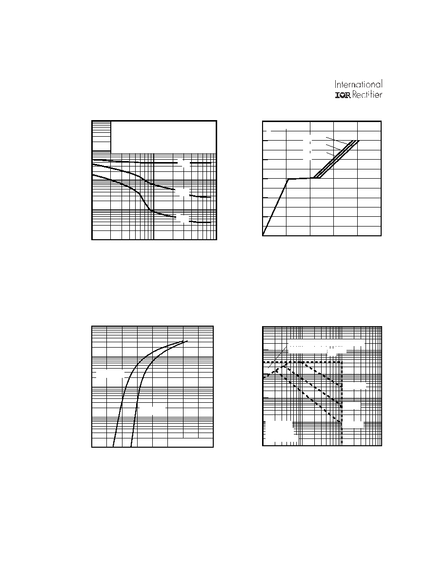
Fig 8. Maximum Safe Operating Area
Fig 6. Typical Gate Charge Vs.
Gate-to-Source Voltage
Fig 5. Typical Capacitance Vs.
Drain-to-Source Voltage
Fig 7. Typical Source-Drain Diode
Forward Voltage
0.1
1
10
100
1000
0.0
0.5
1.0
1.5
2.0
V ,Source-to-Drain Voltage (V)
I
,
R
e
v
e
rs
e D
r
ain C
u
rrent
(A)
SD
SD
V = 0 V
GS
T = 175 C
J
°
T = 25 C
J
°
1
10
100
VDS, Drain-to-Source Voltage (V)
10
100
1000
10000
100000
C
,
C
a
p
a
c
i
t
a
n
c
e
(
p
F
)
VGS = 0V, f = 1 MHZ
Ciss = Cgs + Cgd, Cds SHORTED
Crss = Cgd
Coss = Cds + Cgd
Coss
Crss
Ciss
1
10
100
1000
VDS, Drain-to-Source Voltage (V)
0.1
1
10
100
1000
10000
I D
,
D
r
a
i
n
-
t
o
-
S
o
u
r
c
e
C
u
r
r
e
n
t
(
A
)
Tc = 25°C
Tj = 175°C
Single Pulse
1msec
10msec
OPERATION IN THIS AREA
LIMITED BY R DS(on)
100µsec
0
20
40
60
80
100
QG Total Gate Charge (nC)
0
2
4
6
8
10
12
V
G
S
,
G
a
t
e
-
t
o
-
S
o
u
r
c
e
V
o
l
t
a
g
e
(
V
)
VDS= 80V
VDS= 50V
VDS= 20V
ID= 80A
IRF8010S/IRF8010L
www.irf.com
5
Fig 10a. Switching Time Test Circuit
V
DS
90%
10%
V
GS
t
d(on)
t
r
t
d(off)
t
f
Fig 10b. Switching Time Waveforms
V
DS
Pulse Width
1
µs
Duty Factor
0.1 %
R
D
V
GS
R
G
D.U.T.
10V
+
-
V
DD
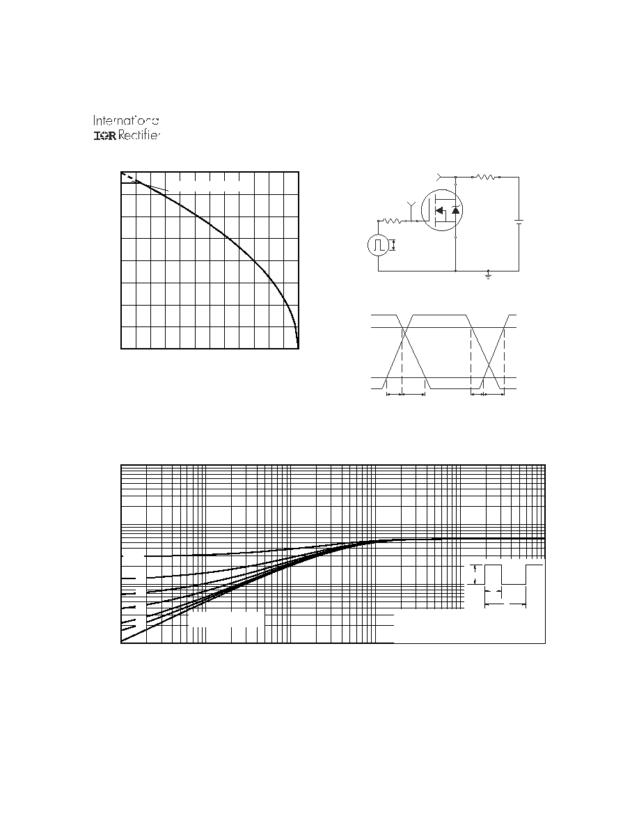
Fig 11. Maximum Effective Transient Thermal Impedance, Junction-to-Case
Fig 9. Maximum Drain Current Vs.
Case Temperature
25
50
75
100
125
150
175
0
20
40
60
80
T , Case Temperature ( C)
I
,
D
r
ai
n C
u
r
r
ent
(
A
)
°
C
D
LIMITED BY PACKAGE
0.01
0.1
1
10
0.00001
0.0001
0.001
0.01
0.1
1
Notes:
1. Duty factor D =
t / t
2. Peak T
= P
x Z
+ T
1
2
J
DM
thJC
C
P
t
t
DM
1
2
t , Rectangular Pulse Duration (sec)
T
her
mal
Res
pons
e
(
Z
)
1
th
JC
0.01
0.02
0.05
0.10
0.20
D = 0.50
SINGLE PULSE
(THERMAL RESPONSE)