Äîêóìåíòàöèÿ è îïèñàíèÿ www.docs.chipfind.ru
www.irf.com
1
01/05/06
IRF7854PbF
HEXFET
®
Power MOSFET
Applications
l
Primary Side Switch in Bridge or two-
switch forward topologies using 48V
(±10%) or 36V to 60V ETSI range inputs.
l
Secondary Side Synchronous
Rectification Switch for 12Vout
l
Suitable for 48V Non-Isolated
Synchronous Buck DC-DC Applications
Benefits
l
Low Gate to Drain Charge to Reduce
Switching Losses
l
Fully Characterized Capacitance Including
Effective C
OSS
to Simplify Design,
(See App. Note AN1001)
l
Fully Characterized Avalanche Voltage
and Current
Notes
through
are on page 8
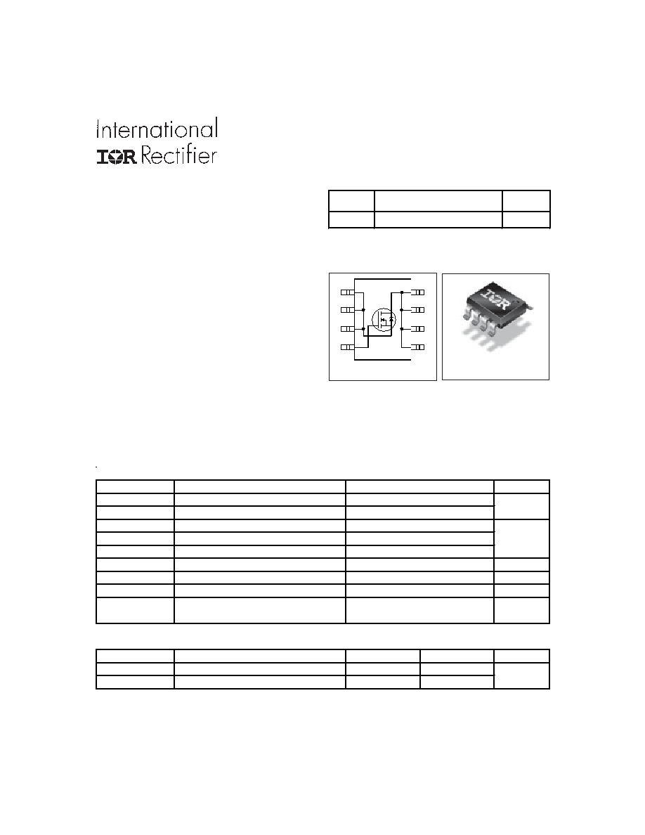
SO-8
Top View
8
1
2
3
4
5
6
7
D
D
D
D
G
S
A
S
S
A
PD - 97172
V
DSS
R
DS(on)
max
I
D
80V
13.4m
:@VGS = 10V 10A
Absolute Maximum Ratings
Parameter
Units
V
DS
Drain-to-Source Voltage
V
V
GS
Gate-to-Source Voltage
I
D
@ T
A
= 25°C
Continuous Drain Current, V
GS
@ 10V
A
I
D
@ T
A
= 70°C
Continuous Drain Current, V
GS
@ 10V
I
DM
Pulsed Drain Current
c
P
D
@T
A
= 25°C
Maximum Power Dissipation
W
Linear Derating Factor
W/°C
dv/dt
Peak Diode Recovery dv/dt
h
V/ns
T
J
Operating Junction and
°C
T
STG
Storage Temperature Range
Thermal Resistance
Parameter
Typ.
Max.
Units
R
JL
Junction-to-Drain Lead
20
°C/W
R
JA
Junction-to-Ambient (PCB Mount)
ei
50
2.5
Max.
10
7.9
79
80
± 20
11
-55 to + 150
0.02
IRF7854PbF
2
www.irf.com
S
D
G
Static @ T
J
= 25°C (unless otherwise specified)
Parameter
Min. Typ. Max. Units
V
(BR)DSS
Drain-to-Source Breakdown Voltage
80
V
V
(BR)DSS
/
T
J
Breakdown Voltage Temp. Coefficient
0.095
V/°C
R
DS(on)
Static Drain-to-Source On-Resistance
11
13.4
m
V
GS(th)
Gate Threshold Voltage
3.0
4.9
V
I
DSS
Drain-to-Source Leakage Current
20
µA
250
I
GSS
Gate-to-Source Forward Leakage
100
nA
Gate-to-Source Reverse Leakage
-100
Dynamic @ T
J
= 25°C (unless otherwise specified)
Parameter
Min. Typ. Max. Units
gfs
Forward Transconductance
12
S
Q
g
Total Gate Charge
27
41
Q
gs
Gate-to-Source Charge
7.7
nC
Q
gd
Gate-to-Drain ("Miller") Charge
8.7
t
d(on)
Turn-On Delay Time
9.4
t
r
Rise Time
8.5
t
d(off)
Turn-Off Delay Time
15
ns
t
f
Fall Time
8.6
C
iss
Input Capacitance
1620
C
oss
Output Capacitance
350
C
rss
Reverse Transfer Capacitance
86
pF
C
oss
Output Capacitance
1730
C
oss
Output Capacitance
230
C
oss
eff.
Effective Output Capacitance
410
Avalanche Characteristics
Parameter
Units
E
AS
Single Pulse Avalanche Energy
d
mJ
I
AR
Avalanche Current
Ã
A
Diode Characteristics
Parameter
Min. Typ. Max. Units
I
S
Continuous Source Current
2.3
(Body Diode)
A
I
SM
Pulsed Source Current
79
(Body Diode)
Ã
V
SD
Diode Forward Voltage
1.3
V
t
rr
Reverse Recovery Time
43
65
ns
Q
rr
Reverse Recovery Charge
76
110
nC
t
on
Forward Turn-On Time
Intrinsic turn-on time is negligible (turn-on is dominated by LS+LD)
Typ.
Conditions
V
DS
= 25V, I
D
= 6.0A
I
D
= 6.0A
V
DS
= 40V
Conditions
V
GS
= 10V
f
V
GS
= 0V
V
DS
= 25V
= 1.0MHz
110
6.0
MOSFET symbol
showing the
integral reverse
p-n junction diode.
T
J
= 25°C, I
S
= 6.0A, V
GS
= 0V
f
T
J
= 25°C, I
F
= 6.0A, V
DD
= 25V
di/dt = 100A/µs
f
Conditions
V
GS
= 0V, I
D
= 250µA
Reference to 25°C, I
D
= 1mA
V
GS
= 10V, I
D
= 10A
f
V
DS
= V
GS
, I
D
= 100µA
V
DS
= 80V, V
GS
= 0V
V
DS
= 80V, V
GS
= 0V, T
J
= 125°C
V
GS
= 20V
V
GS
= -20V
Max.
V
GS
= 0V, V
DS
= 1.0V, = 1.0MHz
V
GS
= 0V, V
DS
= 64V, = 1.0MHz
V
GS
= 0V, V
DS
= 0V to 64V
g
V
GS
= 10V
f
V
DD
= 40V
I
D
= 6.0A
R
G
= 6.2
IRF7854PbF
www.irf.com
3
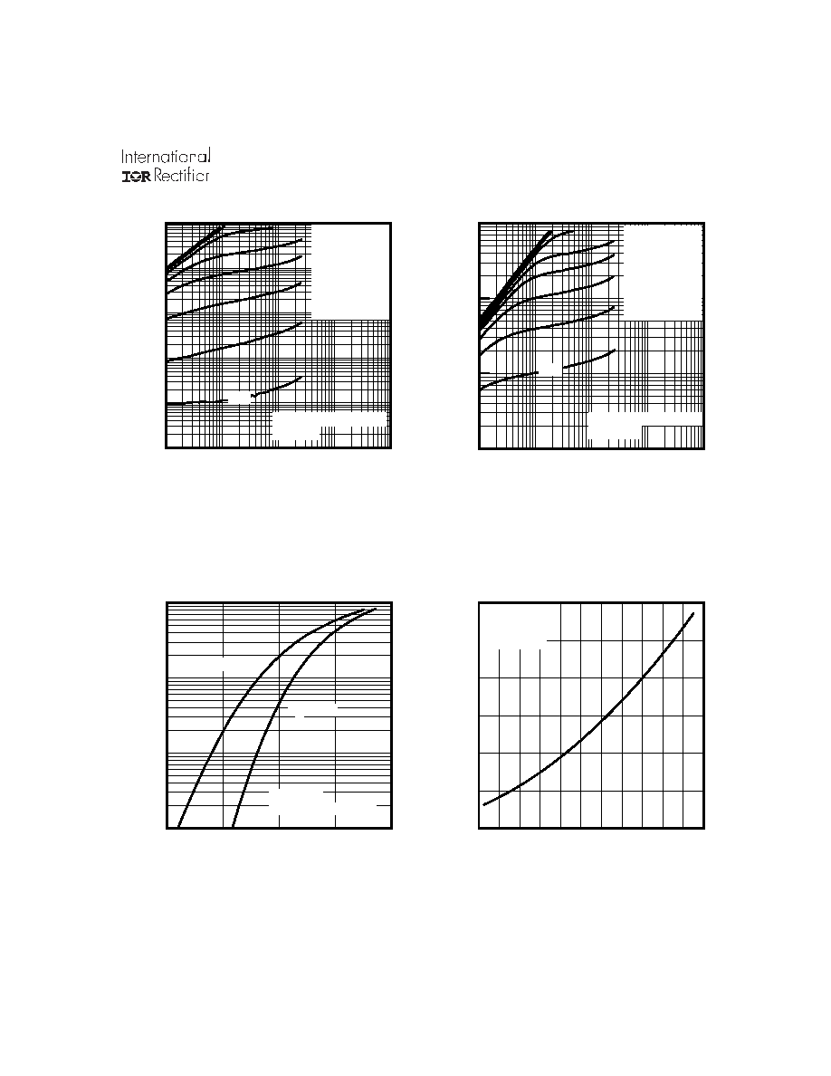
Fig 2. Typical Output Characteristics
Fig 1. Typical Output Characteristics
Fig 3. Typical Transfer Characteristics
Fig 4. Normalized On-Resistance
vs. Temperature
0.1
1
10
100
1000
VDS, Drain-to-Source Voltage (V)
0.1
1
10
100
I D
,
D
r
a
i
n
-
t
o
-
S
o
u
r
c
e
C
u
r
r
e
n
t
(
A
)
5.0V
60µs PULSE WIDTH
Tj = 150°C
VGS
TOP 15V
10V
8.0V
7.0V
6.5V
6.0V
5.5V
BOTTOM
5.0V
0.1
1
10
100
1000
VDS, Drain-to-Source Voltage (V)
0.001
0.01
0.1
1
10
100
I D
,
D
r
a
i
n
-
t
o
-
S
o
u
r
c
e
C
u
r
r
e
n
t
(
A
)
VGS
TOP 15V
10V
8.0V
7.0V
6.5V
6.0V
5.5V
BOTTOM
5.0V
60µs PULSE WIDTH
Tj = 25°C
5.0V
4
5
6
7
8
VGS, Gate-to-Source Voltage (V)
0.1
1
10
100
I D
,
D
r
a
i
n
-
t
o
-
S
o
u
r
c
e
C
u
r
r
e
n
t
(
A
)
TJ = 25°C
TJ = 150°C
VDS = 25V
60µs PULSE WIDTH
-60 -40 -20 0 20 40 60 80 100 120 140 160
TJ , Junction Temperature (°C)
0.5
1.0
1.5
2.0
R
D
S
(
o
n
)
,
D
r
a
i
n
-
t
o
-
S
o
u
r
c
e
O
n
R
e
s
i
s
t
a
n
c
e
(
N
o
r
m
a
l
i
z
e
d
)
ID = 10A
VGS = 10V
IRF7854PbF
4
www.irf.com
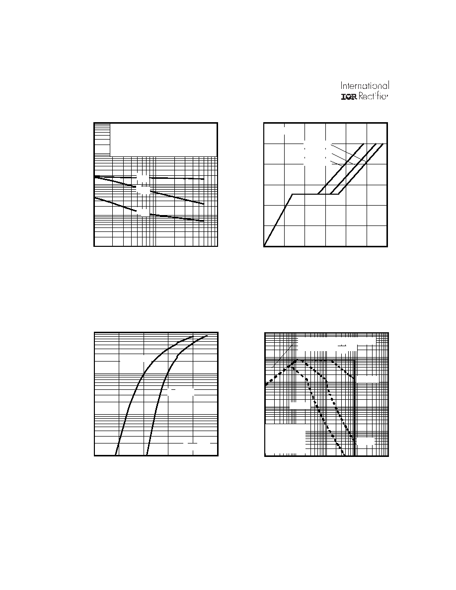
Fig 6. Typical Gate Charge vs.
Gate-to-Source Voltage
Fig 5. Typical Capacitance vs.
Drain-to-Source Voltage
Fig 7. Typical Source-Drain Diode
Forward Voltage
Fig 8. Maximum Safe Operating Area
1
10
100
VDS, Drain-to-Source Voltage (V)
10
100
1000
10000
100000
C
,
C
a
p
a
c
i
t
a
n
c
e
(
p
F
)
VGS = 0V, f = 1 MHZ
Ciss = Cgs + Cgd, C ds SHORTED
Crss = Cgd
Coss = Cds + Cgd
Coss
Crss
Ciss
0.2
0.4
0.6
0.8
1.0
1.2
VSD, Source-to-Drain Voltage (V)
0.1
1
10
100
I S
D
,
R
e
v
e
r
s
e
D
r
a
i
n
C
u
r
r
e
n
t
(
A
)
TJ = 25°C
TJ = 150°C
VGS = 0V
0
1
10
100
1000
VDS, Drain-to-Source Voltage (V)
0.01
0.1
1
10
100
1000
I D
,
D
r
a
i
n
-
t
o
-
S
o
u
r
c
e
C
u
r
r
e
n
t
(
A
)
OPERATION IN THIS AREA
LIMITED BY RDS(on)
TA = 25°C
Tj = 150°C
Single Pulse
100µsec
1msec
10msec
0
5
10
15
20
25
30
QG, Total Gate Charge (nC)
0.0
2.0
4.0
6.0
8.0
10.0
12.0
V
G
S
,
G
a
t
e
-
t
o
-
S
o
u
r
c
e
V
o
l
t
a
g
e
(
V
)
VDS= 64V
VDS= 40V
VDS= 16V
ID= 6.0A
IRF7854PbF
www.irf.com
5
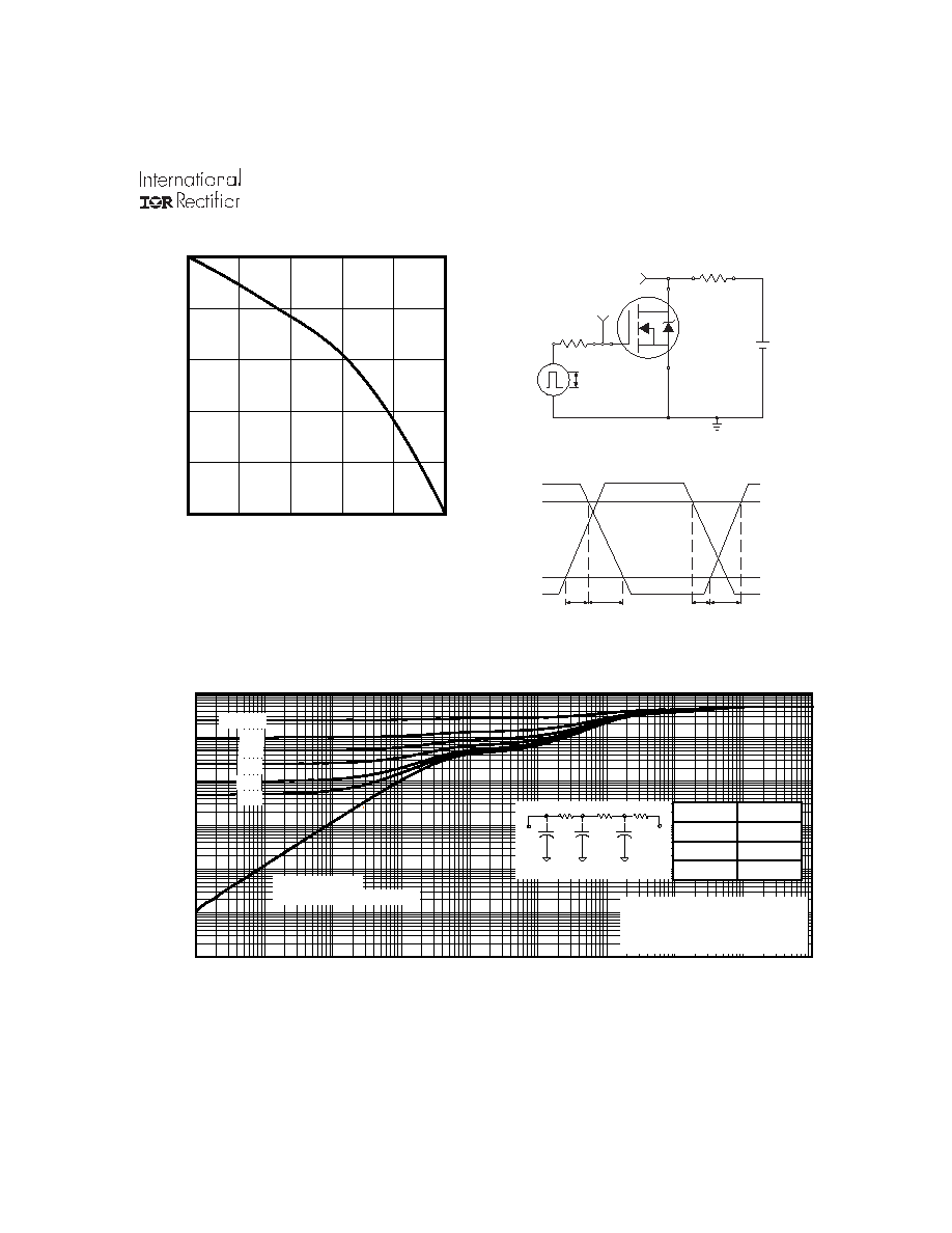
Fig 11. Maximum Effective Transient Thermal Impedance, Junction-to-Ambient
Fig 10a. Switching Time Test Circuit
V
DS
90%
10%
V
GS
t
d(on)
t
r
t
d(off)
t
f
Fig 10b. Switching Time Waveforms
V
DS
Pulse Width 1 µs
Duty Factor 0.1 %
R
D
V
GS
R
G
D.U.T.
10V
+
-
V
DD
Fig 9. Maximum Drain Current vs.
Ambient Temperature
25
50
75
100
125
150
TA , Ambient Temperature (°C)
0
2
4
6
8
10
I D
,
D
r
a
i
n
C
u
r
r
e
n
t
(
A
)
1E-006
1E-005
0.0001
0.001
0.01
0.1
1
10
100
1000
t1 , Rectangular Pulse Duration (sec)
0.0001
0.001
0.01
0.1
1
10
100
T
h
e
r
m
a
l
R
e
s
p
o
n
s
e
(
Z
t
h
J
A
)
0.20
0.10
D = 0.50
0.02
0.01
0.05
SINGLE PULSE
( THERMAL RESPONSE )
Notes:
1. Duty Factor D = t1/t2
2. Peak Tj = P dm x Zthja + Tc
Ri (°C/W)
(sec)
4.329
0.003565
30.099
1.1249
15.590
34.5
J
J
1
1
2
2
3
3
R
1
R
1
R
2
R
2
R
3
R
3
Ci=
i/Ri
Ci=
i/Ri
A