Äîêóìåíòàöèÿ è îïèñàíèÿ www.docs.chipfind.ru
www.irf.com
1
Parameter
Maximum
Units
I
D
@ T
A
= 25°C
Continuous Drain Current, V
GS
@ 4.5V
2.4
A
I
D
@ T
A
= 70°C
1.9
I
DM
Pulsed Drain Current
19
P
D
@T
A
= 25°C
Power Dissipation
1.3
W
P
D
@T
A
= 70°C
0.8
Linear Derating Factor
10
mW/°C
V
GS
Gate-to-Source Voltage
± 12
V
dv/dt
Peak Diode Recovery dv/dt
5.0
V/ns
T
J,
T
STG
Junction and Storage Temperature Range
-55 to +150
°C
q
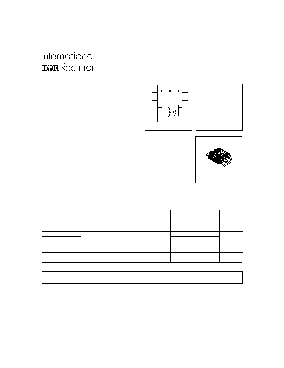
Co-packaged HEXFET
®
Power MOSFET
and Schottky Diode
q
N-Channel HEXFET
q
Low V
F
Schottky Rectifier
q
Generation 5 Technology
q
Micro8
TM
Footprint
IRF7521D1
PRELIMINARY
FETKY
TM
TM
TM
TM
TM
MOSFET / Schottky Diode
Notes:
Repetitive rating; pulse width limited by maximum junction temperature (see figure 9)
I
SD
1.7A, di/dt
66A/µs, V
DD
V
(BR)DSS
, T
J
150°C
Pulse width
300µs; duty cycle
2%
Surface mounted on FR-4 board, t
10sec.
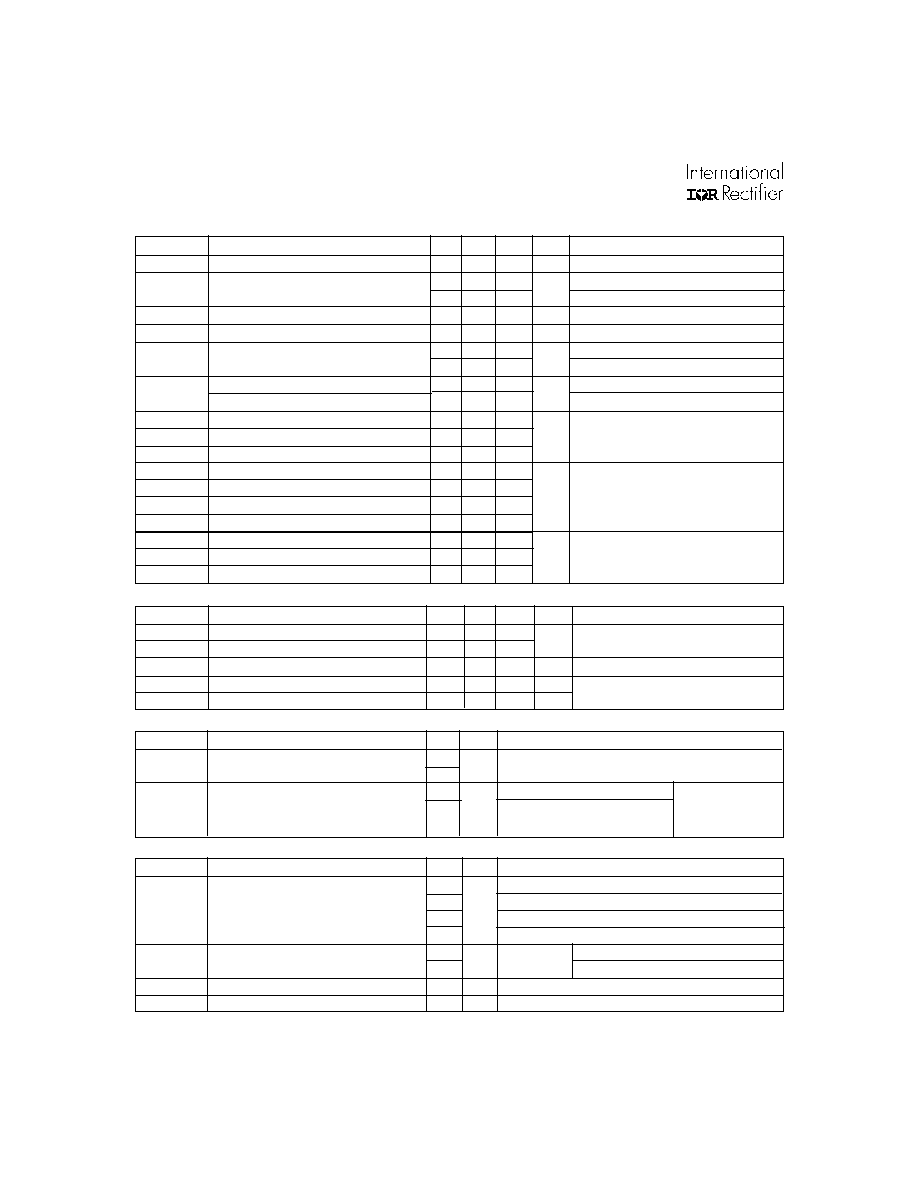
Parameter
Maximum
Units
R
JA
Junction-to-Ambient
100
°C/W
Absolute Maximum Ratings
(T
A
= 25°C unless otherwise noted)
Thermal Resistance Ratings
Description
V
DSS
= 20V
R
DS(on)
= 0.135
Schottky Vf = 0.39V
01/29/99
Micro8
TM
T op V ie w
8
1
2
3
4
5
6
7
A
A
S
G
D
D
K
K
The FETKY
TM
family of co-packaged HEXFETs and Schottky diodes offer the
designer an innovative board space saving solution for switching regulator
applications. Generation 5 HEXFETs utilize advanced processing techniques to
achieve extremely low on-resistance per silicon area. Combining this technology
with International Rectifier's low forward drop Schottky rectifiers results in an
extremely efficient device suitable for use in a wide variety of portable electronics
applications like cell phone, PDA, etc.
The new Micro8
TM
package, with half the footprint area of the standard SO-8,
provides the smallest footprint available in an SOIC outline. This makes the Micro8
TM
an ideal device for applications where printed circuit board space is at a premium.
The low profile (<1.1mm) of the Micro8
TM
will allow it to fit easily into extremely thin
application environments such as portable electronics and PCMCIA cards.
PD-91646C
IRF7521D1
2
www.irf.com
2
Parameter
Min. Typ. Max. Units
Conditions
V
(BR)DSS
Drain-to-Source Breakdown Voltage
20
V
V
GS
= 0V, I
D
= 250µA
0.085 0.135
V
GS
= 4.5V, I
D
= 1.7A
0.12 0.20
V
GS
= 2.7V, I
D
= 0.85A
V
GS(th)
Gate Threshold Voltage
0.70
V
V
DS
= V
GS
, I
D
= 250µA
g
fs
Forward Transconductance
2.6
S
V
DS
= 10V, I
D
= 0.85A
1.0
V
DS
= 16V, V
GS
= 0V
25
V
DS
= 16V, V
GS
= 0V, T
J
= 125°C
Gate-to-Source Forward Leakage
100
V
GS
= 12V
Gate-to-Source Reverse Leakage
-100
V
GS
= -12V
Q
g
Total Gate Charge
5.3
8.0
I
D
= 1.7A
Q
gs
Gate-to-Source Charge
0.84
1.3
nC
V
DS
= 16V
Q
gd
Gate-to-Drain ("Miller") Charge
2.2
3.3
V
GS
= 4.5V, See Fig. 6
t
d(on)
Turn-On Delay Time
5.7
V
DD
= 10V
t
r
Rise Time
24
I
D
= 1.7A
t
d(off)
Turn-Off Delay Time
15
R
G
= 6.0
t
f
Fall Time
16
R
D
= 5.7
,
C
iss
Input Capacitance
260
V
GS
= 0V
C
oss
Output Capacitance
130
pF
V
DS
= 15V
C
rss
Reverse Transfer Capacitance
61
= 1.0MHz, See Fig. 5
MOSFET Electrical Characteristics @ T
J
= 25°C (unless otherwise specified)
R
DS(on)
Static Drain-to-Source On-Resistance
I
DSS
Drain-to-Source Leakage Current
I
GSS
µA
nA
ns
Parameter
Min. Typ. Max. Units
Conditions
I
S
Continuous Source Current(Body Diode)
1.3
I
SM
Pulsed Source Current (Body Diode)
14
V
SD
Body Diode Forward Voltage
1.2
V
T
J
= 25°C, I
S
= 1.7A, V
GS
= 0V
t
rr
Reverse Recovery Time (Body Diode)
39
59
ns
T
J
= 25°C, I
F
= 1.7A
Q
rr
Reverse RecoveryCharge
37
56
nC
di/dt = 100A/µs
A
MOSFET Source-Drain Ratings and Characteristics
Parameter
Max. Units.
Conditions
I
F(av)
Max. Average Forward Current
1.9
50% Duty Cycle. Rectangular Wave, T
A
= 25°C
1.4
Fig.14
T
A
= 70°C
I
SM
Max. peak one cycle Non-repetitive
120
5µs sine or 3µs Rect. pulse
Following any rated
Surge current
11
10ms sine or 6ms Rect. pulse load condition &
with V
RRM
applied
A
A
Schottky Diode Maximum Ratings
Parameter
Max. Units
Conditions
V
FM
Max. Forward voltage drop
0.50
I
F
= 1.0A, T
J
= 25°C
0.62
I
F
= 2.0A, T
J
= 25°C
0.39
I
F
= 1.0A, T
J
= 125°C
0.57
I
F
= 2.0A, T
J
= 125°C .
I
RM
Max. Reverse Leakage current
0.02
V
R
= 20V
T
J
= 25°C
8
T
J
= 125°C
C
t
Max. Junction Capacitance
92
pF
V
R
= 5Vdc ( 100kHz to 1 MHz) 25°C
dv/dt
Max. Voltage Rate of Charge
3600 V/ µs Rated V
R
Schottky Diode Electrical Specifications
V
mA
(
HEXFET
is
the
reg.
TM
for
International
Rectifier
Power
MOSFET's
)
See
IRF7521D1
www.irf.com
3
2
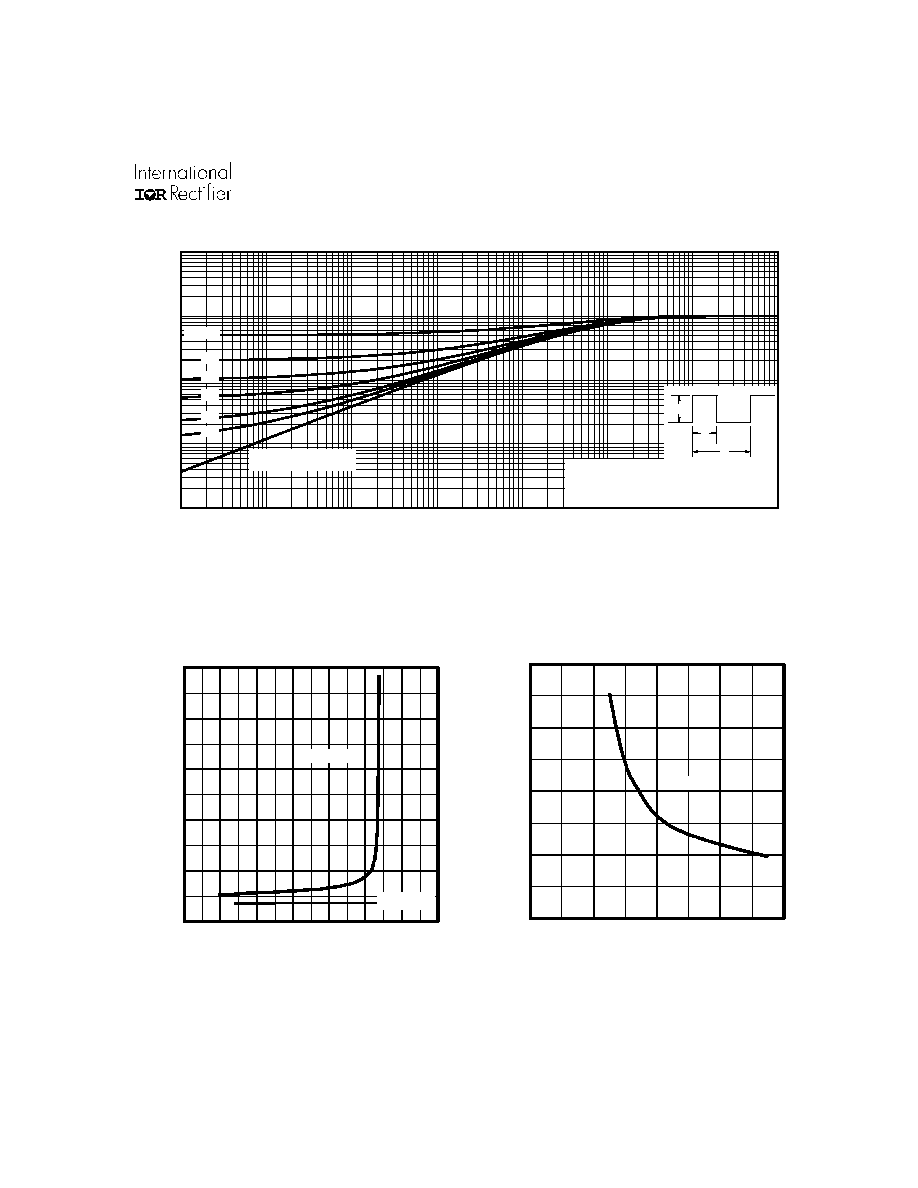
Power Mosfet Characteristics
Fig 4. Normalized On-Resistance
Vs. Temperature
Fig 1. Typical Output Characteristics
Fig 2. Typical Output Characteristics
Fig 3. Typical Transfer Characteristics
0 . 0 1
0.1
1
1 0
1 0 0
0.1
1
1 0
I , D
r
a
i
n
-
to
-
S
o
u
r
c
e
C
u
r
r
e
n
t
(
A
)
D
V , D rain-to-S ourc e V olta ge (V )
D S
20 µ s P U LS E W ID TH
T = 2 5°C
A
VGS
TO P 7.5V
5.0V
4.0V
3.5V
3.0V
2.5V
2.0V
BOT TOM 1.5V
1 .5V
J
0 . 0 1
0.1
1
1 0
1 0 0
0.1
1
1 0
I
,
D
r
ai
n
-
t
o
-
S
ou
r
c
e Cur
r
e
nt
(
A
)
D
V , D rain-to-S ource V oltage (V )
DS
A
VGS
TOP 7.5V
5.0V
4.0V
3.5V
3.0V
2.5V
2.0V
BOTTOM 1.5V
1 .5V
2 0µ s P U L S E W ID T H
T = 15 0°C
J
0 . 1
1
1 0
1 0 0
1 . 5
2 . 0
2 . 5
3 . 0
3 . 5
4 . 0
T = 2 5°C
T = 1 5 0 °C
J
J
G S
V , G ate-to -S o urce V oltag e (V )
D
I
,
D
r
a
i
n
-
to
-
S
o
u
r
c
e
C
u
r
r
e
n
t
(
A
)
A
V = 1 0 V
2 0 µ s P UL S E W ID TH
D S
0.0
0.5
1.0
1.5
2.0
-60
-40
-20
0
2 0
4 0
6 0
8 0
1 0 0 1 2 0 1 4 0 1 6 0
J
T , Junction T em perature (°C )
R
, D
r
a
i
n
-
to
-
S
o
u
r
c
e
O
n
R
e
s
i
s
t
a
n
c
e
DS
(
o
n
)
(
N
or
m
a
l
i
z
ed)
A
V = 4.5 V
G S
I = 1.7A
D
IRF7521D1
4
www.irf.com
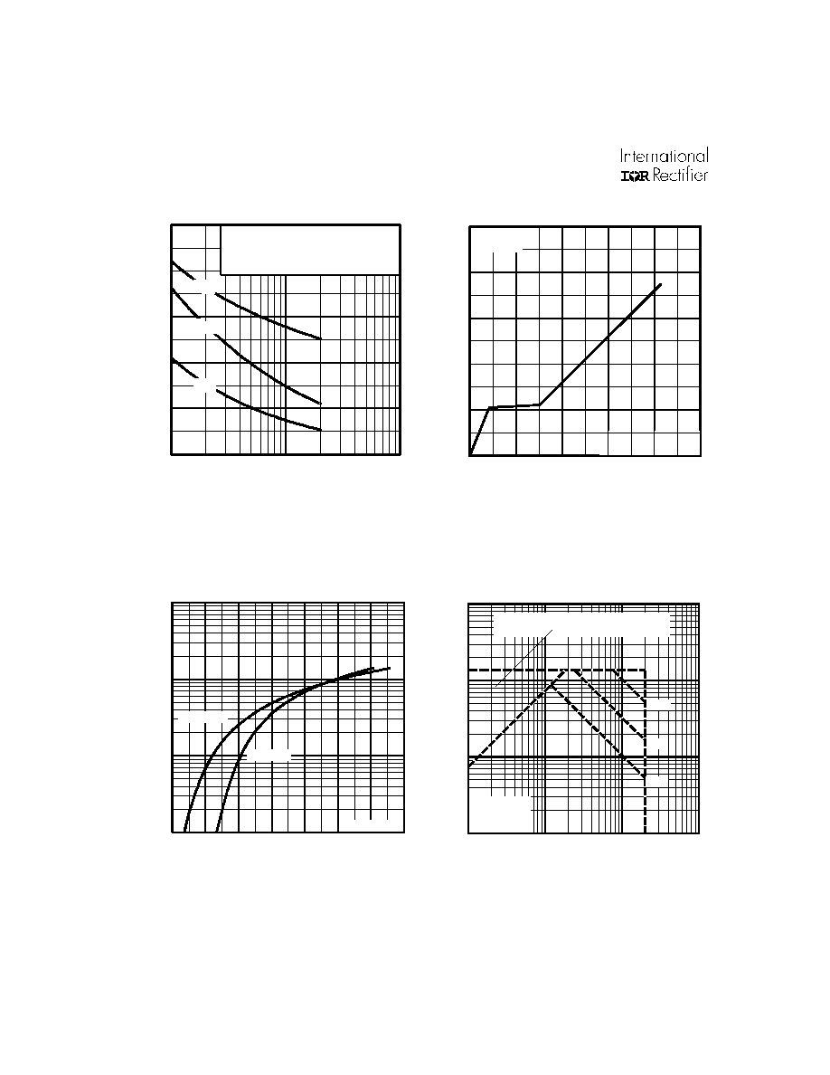
Power Mosfet Characteristics
Fig 7. Typical Source-Drain Diode
Forward Voltage
Fig 6. Typical Gate Charge Vs.
Gate-to-Source Voltage
Fig 5. Typical Capacitance Vs.
Drain-to-Source Voltage
Fig 8. Maximum Safe Operating Area
0
1 0 0
2 0 0
3 0 0
4 0 0
5 0 0
1
1 0
1 0 0
C
,
Cap
ac
i
t
a
n
c
e
(
p
F
)
D S
V , D rain-to-S ourc e V oltage (V )
A
V = 0V , f = 1M H z
C = C + C , C S H O R T E D
C = C
C = C + C
G S
is s g s g d d s
rs s g d
o ss d s gd
C
iss
C
os s
C
rs s
0
2
4
6
8
1 0
0
2
4
6
8
1 0
G
GS
A
-
V
, G
a
te
-
t
o
-
S
o
u
r
c
e
V
o
l
t
a
g
e
(
V
)
Q , Total G ate C harge (nC )
F O R T E S T C IR C U IT
S E E F IG U R E 9
I = 1 .7A
V = 16 V
D
D S
0.1
1
1 0
1 0 0
0.4
0.6
0.8
1.0
1.2
1.4
1.6
1.8
T = 25 °C
T = 1 50 °C
J
J
V = 0V
G S
V , S o urc e-to -D ra in V o lta ge (V )
I , R
e
v
e
r
s
e
D
r
a
i
n
C
u
r
r
e
n
t
(
A
)
S D
SD
A
0.1
1
1 0
1 0 0
0.1
1
1 0
1 0 0
V , D rain-to-S ource V oltage (V )
D S
I
,
Dr
ai
n
C
u
r
r
e
nt
(
A
)
O P E R A T IO N IN T H IS A R E A L IM ITE D
B Y R
D
D S (o n)
T = 25 °C
T = 15 0°C
S ing le P u ls e
1 0 0 µ s
1 m s
1 0 m s
A
A
J
IRF7521D1
www.irf.com
5
Power Mosfet Characteristics
0.1
1
10
100
1000
0.00001
0.0001
0.001
0.01
0.1
1
10
100
Notes:
1. Duty factor D =
t / t
2. Peak T = P
x Z
+ T
1
2
J
DM
thJC
C
P
t
t
DM
1
2
t , Rectangular Pulse Duration (sec)
Thermal Response
(Z )
1
thJC
0.01
0.02
0.05
0.10
0.20
D = 0.50
SINGLE PULSE
(THERMAL RESPONSE)
Fig 9. Maximum Effective Transient Thermal Impedance, Junction-to-Ambient
Fig 10. Typical On-Resistance Vs. Drain
Current
R
DS
(on) , Drain-to-Source On Resistance (
)
Fig 11. Typical On-Resistance Vs. Gate
Voltage
0 . 0
0 . 2
0 . 4
0 . 6
0 . 8
1 . 0
0 . 0
1 . 0
2 . 0
3 . 0
4 . 0
5 . 0
6 . 0
7 . 0
A
I , D rain C urrent (A)
D
V = 2.5V
V = 4.0V
GS
V = 5.0V
GS
0 . 0 4
0 . 0 6
0 . 0 8
0 . 1 0
0 . 1 2
0 . 0
2 . 0
4 . 0
6 . 0
8 . 0
A
G S
V , Gate-to-Source V oltage (V )
I = 1.7A
D
R
DS
(on) , Drain-to-Source On Resistance (
)