www.irf.com
1
11/10/04
IRF6609
HEXFET
«
Power MOSFET
Notes
through are on page 10
l
Low Conduction Losses
l
Low Switching Losses
l
Ideal Synchronous Rectifier MOSFET
l
Low Profile (<0.7 mm)
l
Dual Sided Cooling Compatible
l
Compatible with existing Surface Mount
Techniques
Description
The IRF6609 combines the latest HEXFET« Power MOSFET Silicon technology with the advanced DirectFET
TM
packaging to achieve the
lowest on-state resistance in a package that has the footprint of an SO-8 and only 0.7 mm profile. The DirectFET package is compatible
with existing layout geometries used in power applications, PCB assembly equipment and vapor phase, infra-red or convection soldering
techniques, when application note AN-1035 is followed regarding the manufacturing methods and processes. The DirectFET package
allows dual sided cooling to maximize thermal transfer in power systems, IMPROVING previous best thermal resistance by 80%.
The IRF6609 balances both low resistance and low charge along with ultra low package inductance to reduce both conduction and
switching losses. The reduced total losses make this product ideal for high efficiency DC-DC converters that power the latest generation
of processors operating at higher frequencies. The IRF6609 has been optimized for parameters that are critical in synchronous buck
operating from 12 volt buss converters including Rds(on), gate charge and Cdv/dt-induced turn on immunity. The IRF6609 offers
particularly low Rds(on) and high Cdv/dt immunity for synchronous FET applications.
V
DSS
R
DS(on)
max
Qg
20V
2.0m
@V
GS
= 10V
46nC
2.6m
@V
GS
= 4.5V
Absolute Maximum Ratings
Parameter
Units
V
DS
Drain-to-Source Voltage
V
V
GS
Gate-to-Source Voltage
I
D
@ T
C
= 25░C
Continuous Drain Current, V
GS
@ 10V
I
D
@ T
A
= 25░C
Continuous Drain Current, V
GS
@ 10V
A
I
D
@ T
A
= 70░C
Continuous Drain Current, V
GS
@ 10V
I
DM
Pulsed Drain Current
c
P
D
@T
A
= 25░C
Power Dissipation
g
P
D
@T
A
= 70░C
Power Dissipation
g
W
P
D
@T
C
= 25░C
Power Dissipation
Linear Derating Factor
W/░C
T
J
Operating Junction and
░C
T
STG
Storage Temperature Range
Thermal Resistance
Parameter
Typ.
Max.
Units
R
JA
Junction-to-Ambient
fj
¡¡¡
45
R
JA
Junction-to-Ambient
gj
12.5
¡¡¡
R
JA
Junction-to-Ambient
hj
20
¡¡¡
░C/W
R
JC
Junction-to-Case
ij
¡¡¡
1.4
R
J-PCB
Junction-to-PCB Mounted
1.0
¡¡¡
-40 to + 150
2.8
0.022
1.8
89
Max.
31
25
250
▒20
20
150
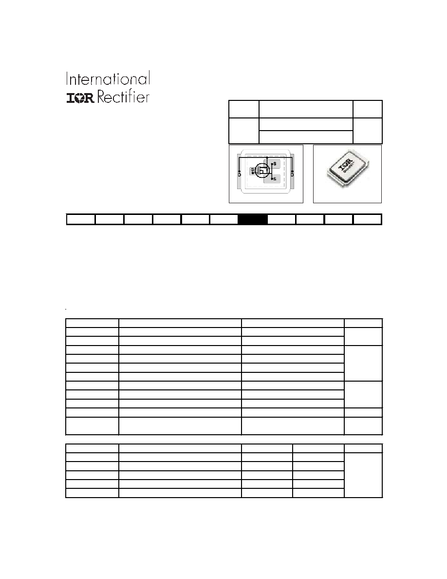
DirectFET
ISOMETRIC
MT
SQ
SX
ST
MQ
MX
MT
Applicable DirectFET Outline and Substrate Outline (see p.8,9 for details)
PD - 95822A

IRF6609
2
www.irf.com
S
D
G
Static @ T
J
= 25░C (unless otherwise specified)
Parameter
Min. Typ. Max. Units
BV
DSS
Drain-to-Source Breakdown Voltage
20
¡¡¡
¡¡¡
V
V
DSS
/
T
J
Breakdown Voltage Temp. Coefficient ¡¡¡
15
¡¡¡ mV/░C
R
DS(on)
Static Drain-to-Source On-Resistance
¡¡¡
1.6
2.0
m
¡¡¡
2.0
2.6
V
GS(th)
Gate Threshold Voltage
1.55
¡¡¡
2.45
V
V
GS(th)
/
T
J
Gate Threshold Voltage Coefficient
¡¡¡
-6.1
¡¡¡ mV/░C
I
DSS
Drain-to-Source Leakage Current
¡¡¡
¡¡¡
1.0
ÁA
¡¡¡
¡¡¡
150
I
GSS
Gate-to-Source Forward Leakage
¡¡¡
¡¡¡
100
nA
Gate-to-Source Reverse Leakage
¡¡¡
¡¡¡
-100
gfs
Forward Transconductance
91
¡¡¡
¡¡¡
S
Q
g
Total Gate Charge
¡¡¡
46
69
Q
gs1
Pre-Vth Gate-to-Source Charge
¡¡¡
15
¡¡¡
Q
gs2
Post-Vth Gate-to-Source Charge
¡¡¡
4.7
¡¡¡
nC
Q
gd
Gate-to-Drain Charge
¡¡¡
15
¡¡¡
Q
godr
Gate Charge Overdrive
¡¡¡
11
¡¡¡
See Fig. 17
Q
sw
Switch Charge (Q
gs2
+ Q
gd
)
¡¡¡
20
¡¡¡
Q
oss
Output Charge
¡¡¡
26
¡¡¡
nC
t
d(on)
Turn-On Delay Time
¡¡¡
24
¡¡¡
t
r
Rise Time
¡¡¡
95
¡¡¡
t
d(off)
Turn-Off Delay Time
¡¡¡
26
¡¡¡
ns
t
f
Fall Time
¡¡¡
9.8
¡¡¡
C
iss
Input Capacitance
¡¡¡
6290
¡¡¡
C
oss
Output Capacitance
¡¡¡
1850
¡¡¡
pF
C
rss
Reverse Transfer Capacitance
¡¡¡
860
¡¡¡
Avalanche Characteristics
Parameter
Units
E
AS
Single Pulse Avalanche Energy
d
mJ
I
AR
Avalanche Current
├
A
Diode Characteristics
Parameter
Min. Typ. Max. Units
I
S
Continuous Source Current
¡¡¡
¡¡¡
31
(Body Diode)
A
I
SM
Pulsed Source Current
¡¡¡
¡¡¡
250
(Body Diode)
├
V
SD
Diode Forward Voltage
¡¡¡
0.80
1.2
V
t
rr
Reverse Recovery Time
¡¡¡
32
48
ns
Q
rr
Reverse Recovery Charge
¡¡¡
26
39
nC
Typ.
¡¡¡
¡¡¡
I
D
= 17A
V
GS
= 0V
V
DS
= 10V
I
D
= 25A
230
25
Max.
T
J
= 25░C, I
F
= 25A
di/dt = 100A/Ás
e
T
J
= 25░C, I
S
= 25A, V
GS
= 0V
e
showing the
integral reverse
p-n junction diode.
Conditions
V
GS
= 0V, I
D
= 250ÁA
Reference to 25░C, I
D
= 1mA
V
GS
= 10V, I
D
= 31A
e
V
GS
= 4.5V, I
D
= 25A
e
V
DS
= V
GS
, I
D
= 250ÁA
V
DS
= 16V, V
GS
= 0V
V
DS
= 16V, V
GS
= 0V, T
J
= 150░C
V
GS
= 20V
V
GS
= -20V
V
GS
= 4.5V
MOSFET symbol
Clamped Inductive Load
V
DS
= 10V, I
D
= 25A
Conditions
= 1.0MHz
V
DS
= 10V, V
GS
= 0V
V
DD
= 16V, V
GS
= 4.5V
├e
V
DS
= 10V

IRF6609
www.irf.com
3
Fig 2. Typical Output Characteristics
Fig 1. Typical Output Characteristics
Fig 3. Typical Transfer Characteristics
Fig 4. Normalized On-Resistance
vs. Temperature
0.1
1
10
100
VDS, Drain-to-Source Voltage (V)
0.1
1
10
100
1000
I D
,
D
r
a
i
n
-
t
o
-
S
o
u
r
c
e
C
u
r
r
e
n
t
(
A
)
60Ás PULSE WIDTH
Tj = 25░C
2.7V
VGS
TOP 10V
7.0V
4.5V
4.0V
3.5V
3.2V
2.9V
BOTTOM
2.7V
0.1
1
10
100
VDS, Drain-to-Source Voltage (V)
1
10
100
1000
I D
,
D
r
a
i
n
-
t
o
-
S
o
u
r
c
e
C
u
r
r
e
n
t
(
A
)
60Ás PULSE WIDTH
Tj = 150░C
2.7V
VGS
TOP 10V
7.0V
4.5V
4.0V
3.5V
3.2V
2.9V
BOTTOM
2.7V
2.0
3.0
4.0
5.0
VGS, Gate-to-Source Voltage (V)
0.1
1.0
10.0
100.0
1000.0
I D
,
D
r
a
i
n
-
t
o
-
S
o
u
r
c
e
C
u
r
r
e
n
t
(
)
VDS = 10V
60Ás PULSE WIDTH
TJ = 25░C
TJ = 150░C
-60 -40 -20
0
20 40 60 80 100 120 140 160
TJ , Junction Temperature (░C)
0.5
1.0
1.5
R
D
S
(
o
n
)
,
D
r
a
i
n
-
t
o
-
S
o
u
r
c
e
O
n
R
e
s
i
s
t
a
n
c
e
(
N
o
r
m
a
l
i
z
e
d
)
ID = 31A
VGS = 10V

IRF6609
4
www.irf.com
Fig 6. Typical Gate Charge vs.
Gate-to-Source Voltage
Fig 5. Typical Capacitance vs.
Drain-to-Source Voltage
Fig 7. Typical Source-Drain Diode
Forward Voltage
Fig 8. Maximum Safe Operating Area
1
10
100
VDS, Drain-to-Source Voltage (V)
100
1000
10000
100000
C
,
C
a
p
a
c
i
t
a
n
c
e
(
p
F
)
Coss
Crss
Ciss
VGS = 0V, f = 1 MHZ
Ciss = Cgs + Cgd, C ds SHORTED
Crss = Cgd
Coss = Cds + Cgd
0
20
40
60
80
100
120
QG Total Gate Charge (nC)
0
2
4
6
8
10
12
V
G
S
,
G
a
t
e
-
t
o
-
S
o
u
r
c
e
V
o
l
t
a
g
e
(
V
)
VDS= 20V
VDS= 10V
ID= 17A
0.0
0.4
0.8
1.2
1.6
2.0
VSD, Source-to-Drain Voltage (V)
0.1
1.0
10.0
100.0
1000.0
I S
D
,
R
e
v
e
r
s
e
D
r
a
i
n
C
u
r
r
e
n
t
(
A
)
TJ = 25░C
TJ = 150░C
VGS = 0V
0
1
10
100
VDS , Drain-toSource Voltage (V)
0.1
1
10
100
1000
I D
,
D
r
a
i
n
-
t
o
-
S
o
u
r
c
e
C
u
r
r
e
n
t
(
A
)
Tc = 25░C
Tj = 150░C
Single Pulse
1msec
10msec
OPERATION IN THIS AREA
LIMITED BY RDS(on)
100Ásec
IRF6609
www.irf.com
5
Fig 11. Maximum Effective Transient Thermal Impedance, Junction-to-Ambient
Fig 10. Threshold Voltage vs. Temperature
Fig 9. Maximum Drain Current vs.
Case Temperature
1E-006
1E-005
0.0001
0.001
0.01
0.1
1
10
100
t1 , Rectangular Pulse Duration (sec)
0.0001
0.001
0.01
0.1
1
10
100
T
h
e
r
m
a
l
R
e
s
p
o
n
s
e
(
Z
t
h
J
A
)
0.20
0.10
D = 0.50
0.02
0.01
0.05
SINGLE PULSE
( THERMAL RESPONSE )
Notes:
1. Duty Factor D = t1/t2
2. Peak Tj = P dm x Zthja + Tc
J
J
1
1
2
2
3
3
R
1
R
1
R
2
R
2
R
3
R
3
Ci i
/Ri
Ci=
i/Ri
C
4
4
R
4
R
4
Ri (░C/W)
i (sec)
0.6784 0.00086
17.299 0.57756
17.566 8.94
9.4701 106
-75
-50
-25
0
25
50
75
100 125 150
TJ , Temperature ( ░C )
1.0
1.5
2.0
2.5
V
G
S
(
t
h
)
G
a
t
e
t
h
r
e
s
h
o
l
d
V
o
l
t
a
g
e
(
V
)
ID = 250ÁA
25
50
75
100
125
150
TJ , Junction Temperature (░C)
0
30
60
90
120
150
I D
,
D
r
a
i
n
C
u
r
r
e
n
t
(
A
)