Äîêóìåíòàöèÿ è îïèñàíèÿ www.docs.chipfind.ru
www.irf.com
1
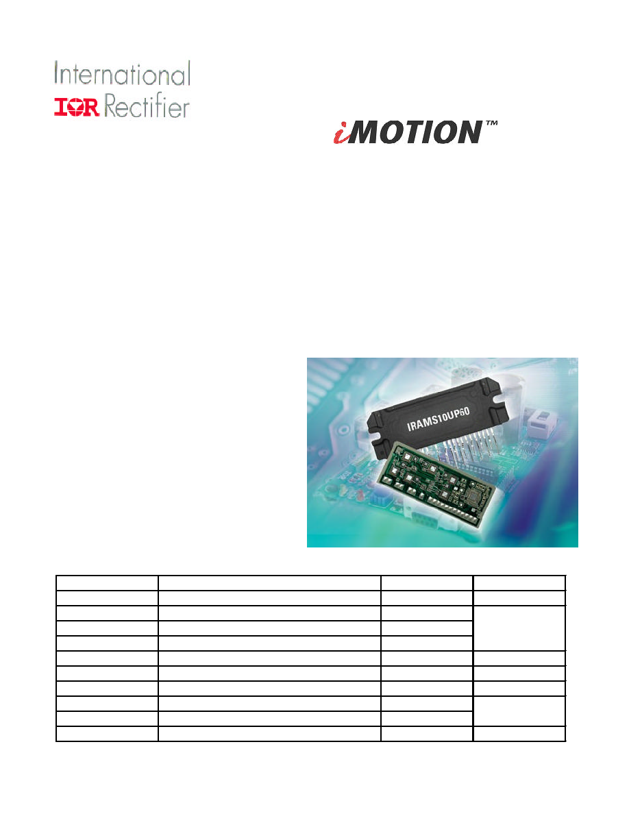
IRAMS10UP60A
Series
Plug N Drive
TM
Integrated Power
Module for Appliance Motor Drive
2/24/03
Features
· Integrated Gate Drivers and Bootstrap Diodes.
· Temperature Monitor
· Temperature and Overcurrent shutdown
· Fully Isolated Package.
· Low VCE (on) Non Punch Through IGBT Technology.
· Undervoltage lockout for all channels
· Matched propagation delay for all channels
· Low side IGBT emitter pins for current conrol
· Schmitt-triggered input logic
· Cross-conduction prevention logic
· Lower di/dt gate driver for better noise immunity
· Motor Power range 0.4~0.75kW / 85~253 Vac
Description
International Rectifier's IRAMS10UP60A is an Integrated Power Module developed and optimized for elec-
tronic motor control in appliance applications such as washing machines and refrigerators. Plug N Drive
technology offers an extremely compact, high performance AC motor-driver in a single isolated package for
a very simple design.
A built-in temperature monitor and over-temperature/over-current protection, along with the short-circuit
rated IGBTs and integrated under-voltage lockout function, deliver high level of protection and fail-safe
operation.
The integration of the bootstrap diodes for the high-side driver section, and the single polarity power
supply required to drive the internal circuitry, simplify the utilization of the module and deliver further cost
reduction advantages.
Absolute Maximum Ratings
Parameter
Description
Max. Value
Units
V
CES
Maximum IGBT Blocking Voltage
600
V
I
o
@ T
C
- 25
o
C
RMS Phase Current
10
I
o
@T
C
- 100
o
C
RMS Phase Current
5
I
pk
Maximum Peak Phase Current (tp<100ms)
15
F
p
Maximum PWM Carrier Frequency
20
kHz
P
d
Maximum Power dissipation per Phase
20
W
V
iso
Isolation Voltage (1min)
2000
V
RMS
T
J
(IGBT & Diodes)
Operating Junction temperature Range
-40 to +150
T
J (Driver IC)
Operating Junction temperature Range
-40 to +150
T
Mounting torque Range (M3 screw)
0.8 to 1.0
Nm
A
°C
PD-94640
IRAMS10UP60A
2
www.irf.com
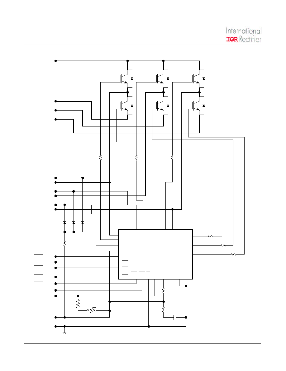
Internal Electrical Schematic - IRAMS10UP60A
23 VS1
24 HO1
25 VB1
1 VCC
2 HIN1
3 HIN2
4 HIN3
5 LIN1
LIN2
6
LIN3
7
F
8
ITRIP
9
EN
10
RCIN
11
VSS
12
COM
13
22
VB2
21
HO2
20
VS2
19
VB3
18
HO3
17
VS3
VRU (12)
VRW (14)
VRV (13)
VB1 (7)
U, VS1 (8)
VB2 (4)
V, VS2 (5)
VB3 (1)
W, VS3 (2)
THERMISTOR
R
3
VDD (22)
VSS (23)
R
1
R
2
C
Rg1
Rg3
Rg5
Driver IC
R
T
LO1 16
LO3 14
LO2 15
Rg2
Rg4
Rg6
T/Itrip (21)
HIN1 (15)
HIN2 (16)
HIN3 (17)
LIN1 (18)
LIN2 (19)
LIN3 (20)
V (10)
+
IRAMS10UP60A
www.irf.com
3
Thermal Resistance
Inverter Section Electrical Characteristics @ T
J
= 25°C
Inverter Section Switching Characteristics @ T
J
= 25°C
Symbol
Param e t e r
M in
Typ
Max
Units Conditions
R
th(J-C)
Junction to case thermal
resistance, each IGBT under
inverter operation.
---
4.2
4.7
°C/W
R
th(J-C)
Junction to case thermal
resistance, each Diode under
inverter operation.
---
5.5
6.5
°C/W
R
th(C-S)
Thermal Resistance case to
sink
---
0.1
---
°C/W
Flat, greased surface.
Heatsink compound thermal
conductivity - 1W/mK
Symbol
Parameter
Min
Typ
Max Units Conditions
V
(BR)CES
Collector-to-Emitter
Breakdown Voltage
600
---
---
V
V
IN
=0V, I
C
=20
µ
A
V
(BR)CES
/
T
Temperature Coeff. Of
Breakdown Voltage
---
0.57
---
V/°C
V
IN
=0V, I
C
=1.0
m
A
(25°C - 150°C)
---
1.7
2.0
I
C
=5A T
J
=25°C, V
DD
=15V
---
2.0
2.4
I
C
=5A T
J
=150°C
---
5
15
V
IN
=5V, V
+
=600V
---
10
40
V
IN
=5V, V
+
=600V, T
J
=150°C
---
1.8
2.35
I
C
=5A
---
1.3
1.7
I
C
=5A, T
J
=150°C
V
µ
A
V
V
CE(ON)
I
CES
V
FM
Collector-to-Emitter Saturation
Voltage
Zero Gate Voltage Collector
Current
Diode Forward Voltage Drop
Symbol
Parameter
Min
Typ
Max Units
E
on
Turn-On Switching Loss
---
155
180
E
off
Turn-Off Switching Loss
---
70
90
E
tot
Total Switching Loss
---
225
270
T
J
=25°C
E
on
Turn-on Swtiching Loss
---
260
300
T
J
=150°C
E
off
Turn-off Switching Loss
---
130
160
E
tot
Total Switching Loss
---
390
460
Erec
Diode Reverse Recovery
energy
---
30
40
µ
J
t
rr
Diode Reverse Recovery time
---
95
110
ns
RBSOA
Reverse Bias Safe Operating
Area
SCSOA
Short Circuit Safe Operating
Area
10
---
---
µ
s
T
J
=150°C, V
P
=600V,
R
G
=33
, V
+
=360V,
V
DD
=+15V to 0V See CT2
µ
J
µ
J
T
J
=150°C, V
+
=400V V
DD
=15V,
I
F
=5A, L=2mH, R
G
=33
FULL SQUARE
T
J
=150°C, I
C
=5A, V
P
=600V
V
+
=480V, V
DD
=+15V to 0V
R
G
=33
See CT3
Conditions
I
C
=5A, V
+
=400V
V
DD
=15V, R
G
=33
, L=2mH
See CT1
Energy losses include "tail" and
diode reverse recovery
IRAMS10UP60A
4
www.irf.com
Recommended Operating Conditions Driver Function
The Input/Output logic timing diagram is shown in figure 1. For proper operation the device should be used within the
recommended conditions. All voltages are absolute referenced to V
SS
. The V
S
offset rating is tested with all supplies biased
at 15V differential. (Note 1)
Static Electrical Characteristics Driver Function
V
BIAS
(V
CC
, V
BS
1,2,3) = 15V unless otherwise specified. The V
IN
and I
IN
parameters are referenced to V
SS
and are
applicable to all six channels. (Note 1)
Absolute Maximum Ratings Driver function
Absolute maximum ratings indicate sustained limits beyond which damage to the device may occur. All voltage param-
eters are absolute voltages referenced to V
SS
. (Note 1)
Sym bol
De finition
M in
Typ
M ax
Units
V
IN,th+
Positive going input threshold
---
---
3
V
V
IN,th-
Negative going input threshold
0.8
---
---
V
I
QBS
Quiescent V
BS
supply current
---
70
120
µ
A
I
QCC
Quiscent V
CC
supply current
---
1.6
2.3
µ
A
I
LK
Offset Supply Leakage Current
---
---
50
µ
A
I
IN+
Input bias current (OUT=HI or OUT=LO)
---
120
---
µ
A
V(T/I
TRIP
)
T/I
TRIP
threshold Voltage (OUT=HI or OUT=LO) (Note 3)
3.85
4.3
4.75
V
11.4
---
V
V
V
10.9
0.2
10.4
---
V
CCUV+
V
BSUV+
V
CCUV-
V
BSUV-
V
CC
and V
BS
supply undervoltage
Negative going threshold
V
CCUVH
V
BSUVH
V
CC
and V
BS
supply undervoltage
I
lockout
hysteresis
10.6
11.1
11.6
V
CC
and V
BS
supply undervoltage
Positive going threshold
14
Symbol
Definition
Min
Max
Units
V
+
High Side offset voltage
-0.3
600
V
V
B1,2,3
High Side floating supply voltage
-0.3
20
V
V
DD
Low Side and logic fixed supply voltage
-0.3
20
V
V
IN
Input voltage LIN, HIN, T/I
TRIP
-0.3
7
V
T
J
Juction Temperature
-40
150
°C
Sym bol
De finition
M in
M ax
Units
V
B1,2,3
High side floating supply voltage
V
S
+12
V
S
+20
V
S1,2,3
High side floating supply offset voltage
Note 2
450
V
DD
Low side and logic fixed supply voltage
12
20
V
ITRIP
T/I
TRIP
input voltage
V
SS
V
SS
+5
V
IN
Logic input voltage LIN, HIN
V
SS
V
SS
+5
V
V
V
IRAMS10UP60A
www.irf.com
5
Note 3: The Maximum recommended sense voltage at the T/I
TRIP
terminal under normal operating
conditions is 3.3V.
Dynamic Electrical Characteristics
V
DD
= V
BS
= V
BIAS
= 15V, I
o
= 1A, V
D
=9V , PWM
in
= 2kHz, VIN
ON
= VIN
,th+,
VIN
OFF
= VIN
,th-
T
A
= 25°C unless otherwise specified.
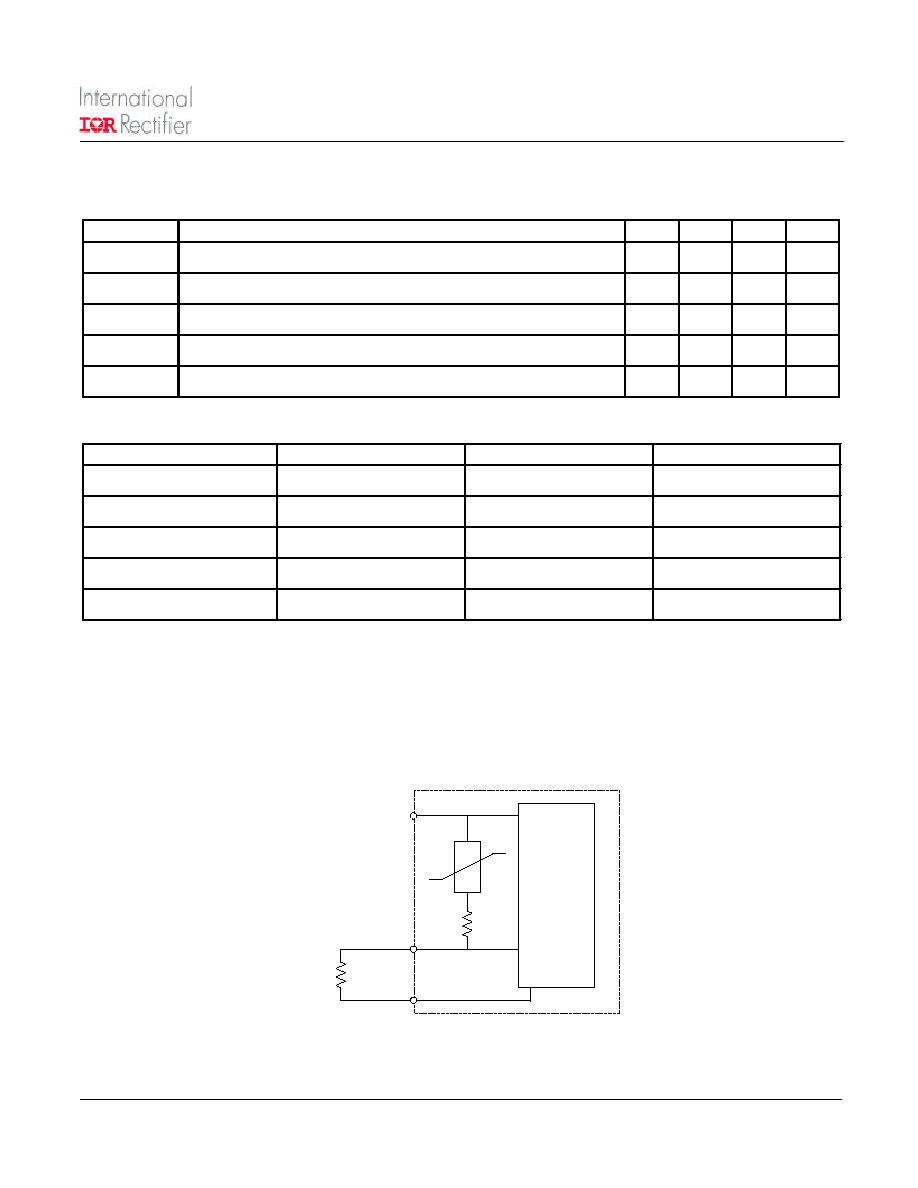
Thermistor Built-in IRAMS10UP60A
Internal NTC - Thermistor Characteristics
Symbol
Definition
Min
Typ
Max Units
T
ON
Input to output propagation turn-on delay time (see fig.11)
-
470
-
ns
T
OFF
Input to output propagation turn-off delay time (see fig. 11)
-
615
-
ns
D
T
Dead Time
-
300
-
ns
I/T
Trip
T/I
Trip
to six switch to turn-off propagation delay (see fig. 2)
-
750
-
ns
T
FCLTRL
Post I
Trip
to six switch to turn-off clear time (see fig. 2)
-
9
-
ms
Typ
Units
Conditions
R
25
Resistance
100 +/- 5%
k
T
C
= 25°C
R
125
Resistance
2.522 + 17.3 % /- 14.9%
k
T
C
= 125°C
R
25/50
Resistance
4250 +/- 3%
k
R
2
= R
1
e
[B(1/T2 - 1/T1)]
-40 / 125
°C
1
mW/°C
T
C
= 25°C
Parameter
Temperature Range
Typ. Dissipation constant
Note 1: For more details, see IR21365 data sheet
Note 2: Logic operational for V
s
from COM-5V to COM+600V. Logic stata held for V
s
from COM-5V to
COM-V
BS
. (please refer to DT97-3 for more details)
VCC (22)
T/I
TRIP
(21)
IR21365
NTC
12K
VSS (23)
4.3K