1
www.irf.com
Junction Size:
Square 370 mils
Wafer Size:
4"
V
RRM
Class:
1200 V
Passivation Process:
Glassivated MESA
Reference IR Packaged Part:
IRKT56 Series
PHASE CONTROL THYRISTORS
IR370BG12DCB
Major Ratings and Characteristics
Parameters
Units
Test Conditions
V
TM
Maximum On-state Voltage
1.2 V
T
J
= 25°C, I
T
= 25 A
V
RRM
Reverse Breakdown Voltage
1200 V
T
J
= 25°C, I
RRM
= 100 µA
(1)
I
GT
Max. Required DC Gate Current to Trigger
150 mA
T
J
= 25° C, anode supply = 6 V, resistive load
V
GT
Max. Required DC Gate Voltage to Trigger
2 V
T
J
= 25° C, anode supply = 6 V, resistive load
I
H
Holding Current Range
5 to 200 mA
Anode supply = 6 V, resistive load
I
L
Maximum Latching Current
400 mA
Anode supply = 6 V, resistive load
Mechanical Characteristics
Nominal Back Metal Composition, Thickness
Cr - Ni - Ag (1 KA - 4 KA - 6 KA)
Nominal Front Metal Composition, Thickness
100% Al, (20 µm)
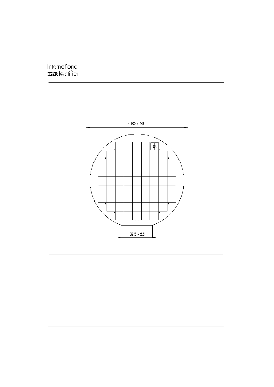
Chip Dimensions
370 x 370 mils (see drawing)
Wafer Diameter
100 mm, with std. <110> flat
Wafer Thickness
370 µm ± 10 µm
Maximum Width of Sawing Line
130 µm
Reject Ink Dot Size
0.25 mm diameter minimum
Ink Dot Location
See drawing
Recommended Storage Environment
Storage in original container, in dessicated
nitrogen, with no contamination
Bulletin I0201J rev. A 02/97
(1)
Nitrogen flow on die edge.

2
www.irf.com
IR370BG12DCB
IR
370
B
G
12
D
CB
1
2
3
1
-
International Rectifier Device
2
-
Chip Dimension in Mils
3
-
Type of Device: B = Wire Bondable SCR
4
-
Passivation Process: G = Glassivated MESA
5
-
Voltage code: Code x 100 = V
RRM
6
-
Metallization: D = Silver (Anode) - Aluminium (Cathode)
7
-
CB
= Probed Uncut Die (wafer in box)
None = Probed Die in chip carrier
4
Device Code
Ordering Information Table
5
Outline Table
All dimensions are in microns (mils)
7
6
Bulletin I0201J rev. A 02/97