Äîêóìåíòàöèÿ è îïèñàíèÿ www.docs.chipfind.ru
Features
·
Load current feedback
·
Programmable over current shutdown
·
Active clamp
·
E.S.D protection
·
Input referenced to Vcc
·
Over temperatue shutdown
·
Reverse battery protection
IR3311(S)
Data Sheet No.PD60210_C
Description
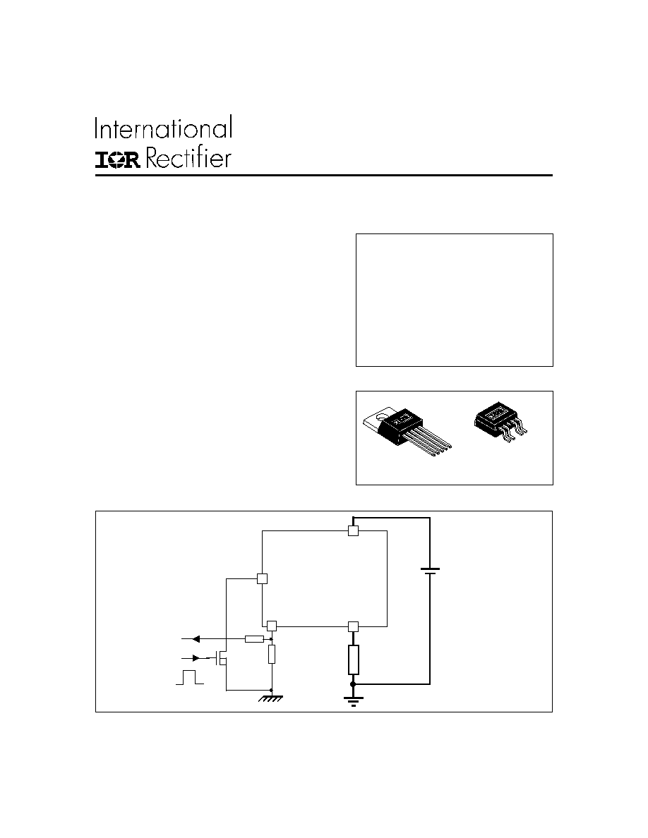
The IR 3311(S) is a Fully Protected 4 terminal high side switch.
The input signal is referenced to Vcc. When the input voltage
Vcc - Vin is higher than the specified Vih threshold, the output
power MOSFET is turned-on. When Vcc - Vin is lower than
the specified Vil threshold, the output MOSFET is turned-off.
A sense current proportional to the current in the power Mosfet
is sourced to the Ifb pin. Over-current shutdown occurs when
Vifb - Vin > 4.5 V. The current shutdown threshold is adjusted
by selecting the proper RIfb. Either over-current and over-tem-
perature latches off the switch. The device is reset by pulling
the input pin high. Other integrated protections ( ESD, reverse
battery, active clamp ) make the IR3311(S) very rugged and
suitable for the automotive environment.
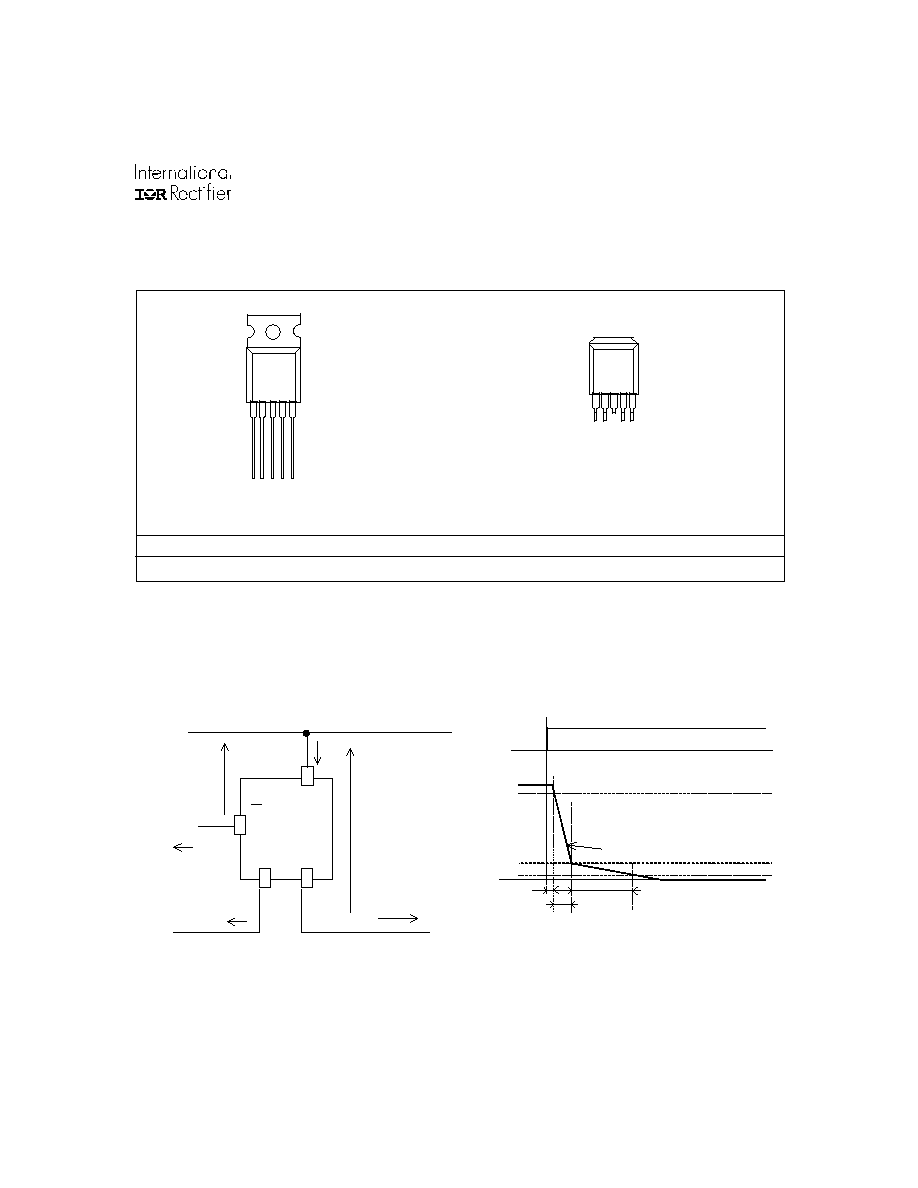
Typical Connection
PROGRAMMABLE CURRENT SENSING HIGH SIDE SWITCH
Product Summary
R
ds(on)
12m
V
cc.op.
6 to 28V
Current ratio
5300
I
shutdown
6A to 58A
Active clamp
35V
Load Dump
40V
Package
www.irf.com
1
VCC
OUT
IN
IR 3311
LOAD
Battery
Power
Ground
System
Ground
off
on
Ifb
10 k
RIfb
5 Lead TO220
IR3311
5 Lead
D
2
Pak (SMD220)
IR3311S
IR3311(S)
2
WWW.IRF.COM
Absolute Maximum Ratings
Absolute maximum ratings indicate sustained limits beyond which damage to the device may occur. All voltage parameters
are referenced to Vcc lead. (TAmbient = 25
o
C unless otherwise specified).
1) Limited by junction temperature. Pulsed current is also limited by wiring
2) <500 Ohm or shorting Ifb to gnd may damage the part with Isd around 90A
3) >5000 Ohm or leaving Ifb open will shutdown the part. No current will flow in the load.
Symbol
Parameter
Min.
Max.
Units
Vcc - Vin max
Maximum input voltage
-16
50
Vcc-VIfb max
Maximum Ifb voltage
-0.3
50
Vcc - Vout max.
Maximum output voltage
-0.3
30
Ids cont.
Diode max. permanent current (Rth = 60 °C/W) (1)
--
2.8
Ids1 cont
Diode max. permanent current (Rth = 5 °C/W) (1)
--
30
Ids pulsed
Diode max. pulsed current (1)
--
100
ESD 1
Electrostatic discharge (human body model) C=100pF, R=1500
,
--
4
ESD 2
Electrostatic discharge (machine model)C=200pF, R=0
,
L=10
µ
H
--
0.5
Pd
Power dissipation ( Rth = 60 °C/W )
--
2
W
TJ max.
Max. storage and junction temperature
-40
150
°C
Min RIfb
Minimum resistor on the Ifb pin
0.3
--
k
Ifb max
Max. Ifb current
-20
+20
mA
V
A
kV
Recommended Operating Conditions
These values are given for a quick design. For operation outside these conditions, please consult the application notes.
Symbol
Parameter
Min.
Max.
Units
Vcc -Vin
Continuous input voltage
6
28
Vcc -VIfb
Continuous Ifb pin voltage
0.3
28
Vcc
Supply to power ground voltage
6
28
Iout
Continuous output
current ( Rth/amb < 5 °C/W, Tj = 125°C)
--
18
Iout 85°C amb.
Continuous output
current ( Rth/amb < 60 °C/W, Tj = 125°C)
-- 5
RIfb
Ifb resistor to program Isd and scale (2 & 3)
0.5 3.5
k
Pulse min.
Minimum turn-on pulse width
1
--
ms
Fmax
Maximum operating frequency
-- 500
Fmax Prot.
Maximum frequency with protections activated
-- 200
V
A
Hz
Thermal Characteristics
Symbol
Parameter
Typ.
Max.
Units
Rth 1
Thermal resistance junction to Ambient - TO220
60
--
Rth 2
Thermal resistance junction to case - TO220
0.7
--
Rth 1
Thermal resistance with standard footprint - SMD220
60
--
Rth 2
Thermal resistance with 1" square footprint - SMD220
35
--
Rth 3
Thermal resistance junction to case - SMD220
0.7
--
°C/W
IR3311(S)
WWW.IRF.COM
3
Symbol Parameter
Min. Typ. Max. Units Test Conditions
Tdon
Turn-on delay time to Vcc-Vout= 0.9 Vcc
2
9
20
Tr1
Rise time to Vcc-Vout=5V
0.4
1.6
5
Tr2
Rise time to Vcc -Vout = 0.1Vcc
10
30
100
Eon
Turn ON energy
--
1.5
3
mJ
Tdoff
Turn-off delay to Vcc -Vout = 0.1Vcc
6
25
80
Tf
Fall time to Vcc-Vout = 0.9 Vcc
3
10
30
Eoff
Turn OFF energy
--
1
2
mJ
see figure 2
µ
s
see figure 3
µ
s
Switching Electrical Characteristics
Vcc = 14V, Resistive Load = 0.4
, T
j
= 25
o
C, (unless otherwise specified).
4) Input thresholds are measured directly between the input pin and the tab. Any parasitic resistance in common between the load
current path and the input signal path can significantly affect the thresholds.
5) Rds(on) is measured between the Tab and the Out pin, 5mm away from the package.
Protection Characteristics
Tj = 25
o
C (unless otherwise specified), RIfb = 500 to 5kOhm.
Symbol
Parameter
Min.
Typ.
Max. Units Test Conditions
VIfb -Vin
@ Isd
Over-current shutdown threshold
4
4.5
5.4
V
Tsd
Over-temp. shutdown threshold
--
165
--
°C
see Fig. 7
Treset
Protection reset time
--
50
300
µ
S
see Fig. 7
OV
Over voltage shutdown (not latched)
--
36
--
V
Isdf
Fixed over current shutdown
58
70
90
A
VIfb<Vin
Isd_1k
Adjustable over current shutdown 1K
18
24
31
A
RIfb=1k
Min.Pulse
Minimum pulse width (no WAIT state)
200
500
1200
µ
s
see Fig. 6
WAIT
WAIT function timer
0.5
1.2
3.5
m
s
see Figs. 6 and 7
Rev.Rdson Rds(on) reverse battery protection
6
10
18
m
Vcc-Vin=-12V, Iload=10A
Symbol
Parameter
Min.
Typ.
Max. Units Test Conditions
Iq
Total quiescent current (Iout +Ifb)
--
22
50
µ
A
Vcc-Vin=0, Vcc-
Vcc-VIfb=12V
Iin
Input current
1.5
4
6
mA
Vcc-Vin=14V
Vih
High level input threshold voltage (4)
--
5
5.5
Vil
Low level input threshold voltage (4)
3.5
4
--
Vhys
Input hysterisis = Vih-Vil
0.4
1
1.5
Iout qs
Output quiescent current
--
9
15
µ
A
Vcc-Vin=0; Vcc-VIfb=0;
Vcc-Vout=12V
Rds1 on
ON state resistance (5)
5
9
12
Iout=30A, Vcc-Vin=14V
Rds2 on
ON state resistance (5)
5
9.5
17
Iout=17A, Vcc -Vin=6V
Rds3 on
ON state resistance (5)
10
17
23
Iout=30A, Tj = 150
o
C
Vclamp1
Vcc to Vout active clamp voltage
30
35
--
Iout = 10mA
Vclamp2
Vcc to Vout active clamp voltage
--
36
40
Iout=30A,Vcc-VIfb<20V
Vsd
Body diode forward voltage
--
0.85
1
Iout=5A
Vaval.
Vcc to Vout avalanche voltage
40
43
50
Iout=100mA,Vcc-Vfb>
Static Electrical Characteristics
(Tj = 25
o
C, Vcc = 14V unless otherwise specified.)
Vout=12V
V
m
V
35V
IR3311(S)
4
WWW.IRF.COM
Functional Block Diagram
Symbol Parameter
Min.
Typ.
Max. Units Test Conditions
Ratio
I load / IIfb current ratio
4,500
5,300
6,300
--
T
j
= 25
o
C ,Rfb = 500
,
I = 50A
Ratio_TC Iload/Ifb variation over temperature
-5
0
+5
%
T
j
= -40 T
0
+150
o
C
offset
Load current diagnostic offset
-0.9
0
0.9
A
I = 2A
Trst
Ifb response time (low signal)
--
0
15
µ
s
90% of the I load step
Current Sense Characteristics
4mA
70V
active clamp
disconnection
-
+
charge
pump
fast turn-off
driver
-
+
4V
reverse
battery
protection
Tj > 165 °C
I out > 60 A
IN
Ifb
OUT
VCC
On/Off
Set
Reset
latch
-
+
Q
timer
1.5 ms
timer
300 us
Wait
33V
Min. pulse
80
70V
33V
33V
43V
36V
IR3311(S)
WWW.IRF.COM
5
Vcc
10 %
Td on
Tr1
Vcc-Vout
Vcc-Vin
90%
Tr2
DV/dt(on)
5V
Figure 1 - Voltages and currents definitions
Figure 2 - Switching time definitions (turn-on)
IR3311
Vcc-Vin
Vcc-Vin
max
Vcc-Vin1
max
Vcc-Vin (op)
Vih
Vil
Vhys
Iin
Iin
max
Iin1,2
Iin(on)
Vcc-Vout
Vcc-Vout
max
Vclamp1
Vclamp2
Iout
Iout
max
-Ids
cont.
-Ids
pulsed
Iout
85°C
Isd
Iq
Vcc
In
Out
Ifb
VIfb
Ifb
Lead Assignments
Part Number
1 2 3 4 5
5 Lead - TO220
IR3311
3 (Vcc)
5 Lead - D
2
PAK (SMD220)
IR3311S
3 (Vcc)
1 2 3 4 5
1 - In
2 - Ifb
3 - Vcc (tab)
4 - NC
5 - Out