
www.irf.com
1
Features
· Output Power FredFET in Half-Bridge Configuration
· High Side Gate Drive Designed for Bootstrap Operation
· Bootstrap Diode Integrated into Package
· Lower Power Level-Shifting Circuit
· Lower di/dt Gate Drive for Better Noise Immunity
· Excellent Latch Immunity on All Inputs and Outputs
· ESD Protection on All Leads
· Isolation 1500 V
RMS
min.
IR3103
Series
0.75A, 500V
Half-Bridge FredFET
and Integrated Driver
Description
The IR3103 is a gate driver IC integrated with a half bridge FredFET designed for motor drive applications
up to 180W (heatsink-less). The sleek and compact single-in-line package is optimized for electronic motor
control in appliance applications such as fans and compressors for refrigerators. The IR3103 offers an
extremely compact, high performance half-bridge inverter in a single isolated package for two-phase and
three-phase motor drivers.
Proprietary HVIC and latch immune CMOS technologies, along with the HEXFET
®
power FredFET
technology (HEXFET
®
MOSFET with ultra-fast recovery body diode characteristics), enable efficient and
rugged single package construction. Propagation delays for the high and low side power FredFETs are
matched thanks to advanced IC technology.
PD-96992 Rev.A
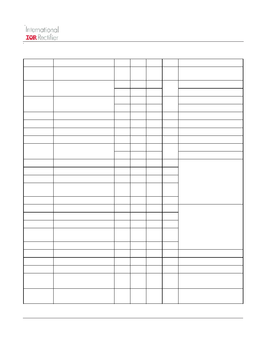
Parameter
Description
Max. Value
Units
V
DS
Drain to Source Blocking Voltage
500
V
V
DD
DC Bus Supply Voltage (No Switching Operation)
500
V
I
O
(T
A
=25°C)
Continuous Output Current (1)
0.7
A
I
O
(T
A
=55°C)
Continuous Output Current (1)
0.6
A
I
O
(T
A
=25°C)
Pulsed Output Current (2)
2.7
A
P
d
Package Power Dissipation @T
A
55°C (3)
1.4
W
V
ISO
Isolation Voltage (1min)
1500
V
RMS
T
J
Junction Temperature (Power MOSFET)
-40 to +150
°C
T
S
Storage Temperature
-40 to +150
°C
T
L
Lead Temperature (soldering, 10 seconds)
300
°C
T
S
Storage Temperature
-40 to +150
°C
Absolute Maximum Ratings
Absolute maximum ratings indicate sustained limits beyond which damage to the device may occur. All voltage
parameters are absolute voltages referenced to COM. Power dissipation is measured under board mounted and still air
conditions.
Note 1: See figure 3, f
PWM
=16kHz
Note 2: T
P
=100ms, other conditions as per Figure 3, f
PWM
=16kHz
Note 3: Single Device Operating

IR3103
2
www.irf.com
Symbol Parameter
Min
Max
Units Conditions
I
BDF
Bootstrap Continuous Diode
Forward Current
---
0.3
A
T
J
= 150°C, T
A
=55°C
V
B
High Side Floating Supply
Absolute Voltage
-0.3
525
V
V
O
High Side Floating Supply Offset
Voltage
V
B
- 25
V
B
+0.3
V
V
CC
Low Side and Logic Fixed Supply
Voltage
-0.3
25
V
V
IN
Input Voltage L
IN
, H
IN
V
SS
-0.3
V
CC
+0.3V
V
V
SS
Logic Ground
V
CC
-25
V
CC
+0.3V
V
Absolute Maximum Ratings (Continued)
Absolute maximum ratings indicate sustained limits beyond which damage to the device may occur. All voltage parameters
are absolute voltages referenced to COM.
Symbol Definition
Min
Max
Units
V
B
High Side Floating Supply Absolute Voltage
V
O
+10
V
O
+20
V
V
DD
High Voltage Supply
Note 4
400
V
V
CC
Low Side and Logic Fixed Supply Voltage
10
20
V
V
IN
Logic Input Voltage
V
SS
V
CC
V
V
SS
Logic Ground
-5
5
V
Recommended Operating Conditions Driver Function
For proper operation the device should be used within the recommended conditions. All voltages are absolute
referenced to COM. The V
S
and V
O
offset are tested with all supplies biased at 15V differential.
Note 4: Logic operation for V
O
of -5 to +500V. Logic state held for V
O
of -5V to -V
BO
. (Please refer to the Design Tip
DT97-3 for more details).
IR3103
www.irf.com
3
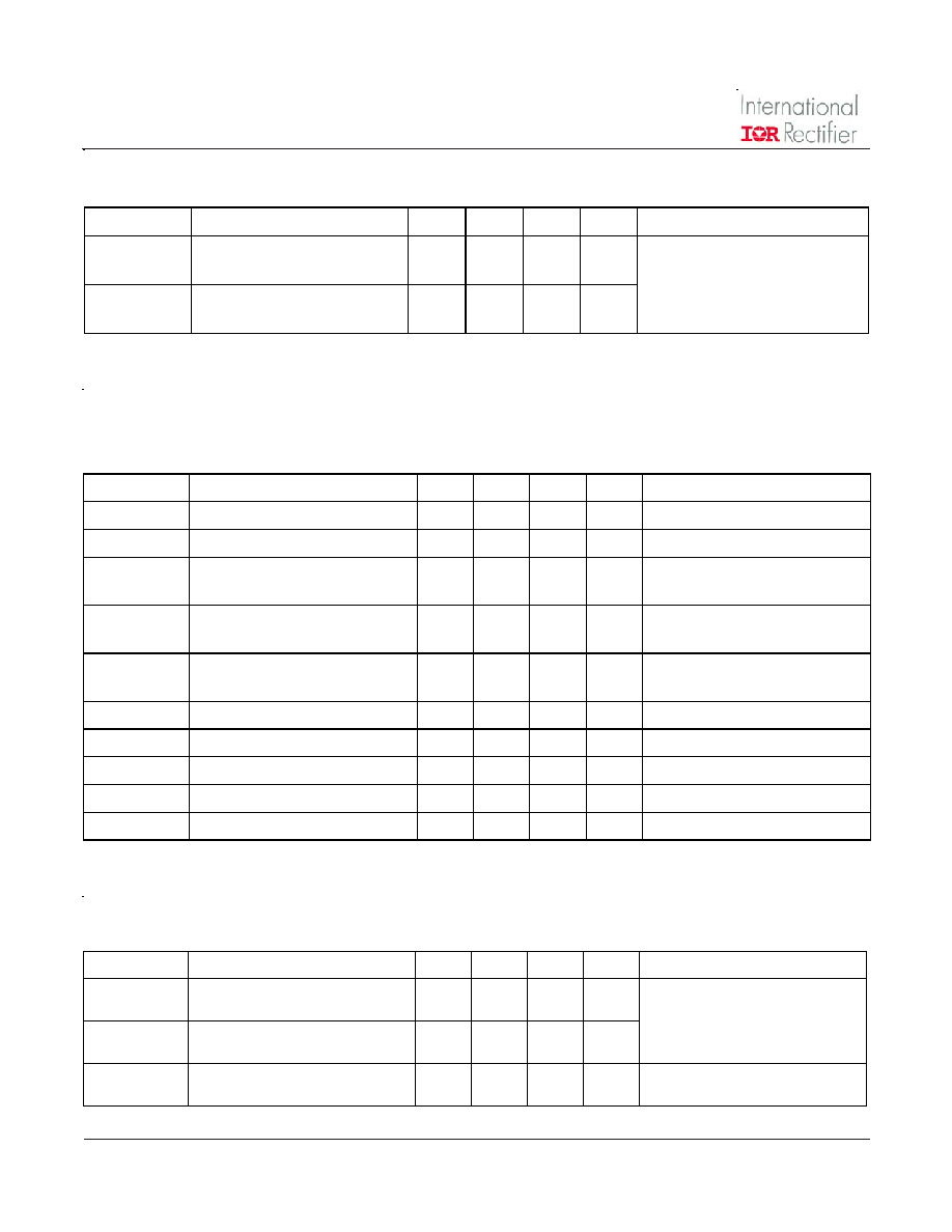
Symbol Parameter
Min
Typ
Max
Units
V
(BR)DSS
Drain-to-Source Breakdown
Voltage
500
---
---
V
V
IN
=0V, I
DD
/I
O
=250µA
---
5
50
V
DS
=500V, V
IN
=0V
---
80
---
V
DS
=500V, V
IN
=0V, T
J
=150°C
---
5
105
V
DS
=500V, V
IN
=0V
---
100
---
V
DS
=500V, V
IN
=0V, T
J
=150°C
R
DS(ON)
Drain-to-Source ON Resistance
---
1.9
2.5
I
O
= 0.75A, V
IN
=5V
V
SD
Diode Forward Voltage
---
0.8
0.9
V
I
O
= 0.75A, V
IN
=0V
R
DS(ON)
Drain-to-Source ON Resistance
---
4.3
6.5
I
O
= 0.75A, V
IN
=5V, T
J
=150°C
V
SD
Diode Forward Voltage
---
0.6
0.75
V
I
O
= 0.75A, V
IN
=0V, T
J
=150°C
---
---
1.25
---
---
1.10
E
ON
Turn-On Energy Losses
---
55
75
µJ
E
OFF
Turn-Off Energy Losses
---
4
10
µJ
E
TOT
Total Energy Losses
---
59
85
µJ
E
REC
Body-Diode Reverse Recovery
Losses
---
2
5
µJ
t
RR
Reverse Recovery Time
---
70
---
ns
E
ON
Turn-On Energy Losses
---
85
115
µJ
E
OFF
Turn-Off Energy Losses
---
5
11
µJ
E
TOT
Total Energy Losses
---
90
126
µJ
E
REC
Body-Diode Reverse Recovery
Losses
---
6
11
µJ
t
RR
Reverse Recovery Time
---
90
---
ns
Q
G
Turn-ON MOSFET Gate Charge
---
15
21
nC
C
OSS
Output Capacitance
---
12
---
pF
C
OSS
eff.
Effective Output Capacitance
---
30
---
pF
SCSOA
Short Circuit Safe Operating
Area
10
---
---
µs
I
SC
Short Circuit Drain Current
---
18.5
---
A
µA
µA
I
HS-LK
I
LS-LK
Low Side Leakage Current
Low Side Leakage Current
I
F
=1A, T
J
=125°C
Note 5: Characterized on FREDFET die level, not measured at EOL
Note 6: C
OSS
eff. is a fixed capacitance that gives same charging time as C
OSS
while V
DS
is rising from 0 to 80% V
DSS
.
V
DD
=400V, f=1MHz. Note 5
V
BDFM
Bootstrap Diode Forward
Voltage Drop
V
Half Bridge Electrical Characteristics @T
J
= 25°C
V
CC
=V
BO
=15V and T
J
=25°C unless otherwise specified. V
DD
and V
IN
parameters referenced to COM
Conditions
I
DD
/I
O
= 0.75A, V
DD
=300V,
V
BO
/V
CC
=15V, L= 6.3mH
Energy Losses include Body-Diode
Reverse Recovery
T
J
=150°C, V
P
=450V,
V
+
= 320V,V
CC
=+15V
T
J
=150°C, V
P
=450V, t
SC
<10µs
V
+
= 320V, V
GE
=15V, V
CC
=+15V
I
DD
/I
O
= 0.75A, V
DD
=300V,
V
BO
/V
CC
=15V, L=6.3mH
T
J
=150°C
Energy Losses include Body-Diode
Reverse Recovery
V
DD
=0V to 400V. Note 5,6
V
DD
=250V, I
O
=3.2A. Note 5
I
F
=1A
IR3103
4
www.irf.com
Symbol Definition
Min
Typ
Max
Units Conditions
T
ON
Input to Output Propagation Turn-
on Delay Time (see fig. 2)
---
300
---
ns
T
OFF
Input to Output Propagation Turn-
off Delay Time (see fig. 2)
---
400
---
ns
M
T
Matching Propagation Delay Time
(On & Off)
---
0
30
ns
V
CC
= V
BO
= 15V
V
CC
=V
BO
= 15V, I
O
=0.75A,
V
DD
=300V
Dynamic Electrical Characteristics Driver Function
Driver only timing unless otherwise specified.
Symbol Parameter
Min
Typ
Max
Units Conditions
Rth
JA self
Self Thermal resistance,
junction to ambient (note 7,8)
---
---
70
°C/W
Rth
JA mutual
Mutual Thermal resistance,
junction to ambient (note 7,8)
---
---
45
°C/W
No airflow
Thermal Resistance
Thermal Resistance is measured under board mounted and still air conditions.
Note 7: under normal operational conditions: both power devices working, no heatsink
Note 8: TJ=RthJA_self*PA+RthJA_mutual*PB
Symbol Definition
Min
Typ
Max
Units
Conditions
V
IN,th
Logic "1" Input Voltage
2.9
---
---
V
V
IN,th
Logic "0" Input Voltage
---
---
0.8
V
V
CCUV+
V
BO
V
CC
and V
BO
Supply Undervoltage
Positive Going Threshold
8.0
8.9
9.8
V
V
CCUV-
V
BO
V
CC
and V
BO
Supply Undervoltage
Negative Going Threshold
7.4
8.2
9.0
V
V
CCUVH
V
BO
V
CC
and V
BO
Supply Undervoltage
Lock-Out Hysteresis
0.3
0.7
---
V
I
LK
Offset Supply Leakage Current
---
---
50
µA
V
B
=V
O
=600V
I
QBS
Quiescent V
BO
Supply Current
---
75
130
µA
V
IN
=0V to 5V
I
QCC
Quiescent V
CC
Supply current
---
120
180
mA
V
IN
=0V to 5V
I
IN+
Input Bias Current
---
5
20
µA
V
IN
=0V to 5V
I
IN-
Input Bias Current
---
---
2
µA
V
IN
=0V
Static Electrical Characteristics Driver Function
V
BIAS
(V
CC
, V
O
)=15V, V
SS
=COM and T
A
=25°C, unless otherwise specified. V
DD and
V
IN
parameters are referenced to COM.

IR3103
www.irf.com
5
1
11
IC Driver
V
o
V
DD
V
B
V
CC
H
IN
L
IN
V
SS
COM
9
11
8
1
2
3
5
6
H
IN
L
IN
V
O
0
1
0
1
0
V
DD
1
1
Shoot-Through
condition
X
X
X
Pin-Out Description
Pin
Name
Description
1
V
CC
Logic and Internal Gate Drive Supply
2
H
IN
Logic Input for High Side Gate Output
3
L
IN
Logic Input For Low Side Gate Output
4
NC
Not Connected
5
V
SS
Logic Ground
6
COM
Low Side MOSFET Gate Return
7
NC
Not Connected
8
V
B
High Side Gate Drive Floating Supply
9
V
O
Half Bridge Output
10
NC
Not Connected
11
V
DD
High Voltage Supply
Figure 1: Driver Input/Output relation