Äîêóìåíòàöèÿ è îïèñàíèÿ www.docs.chipfind.ru
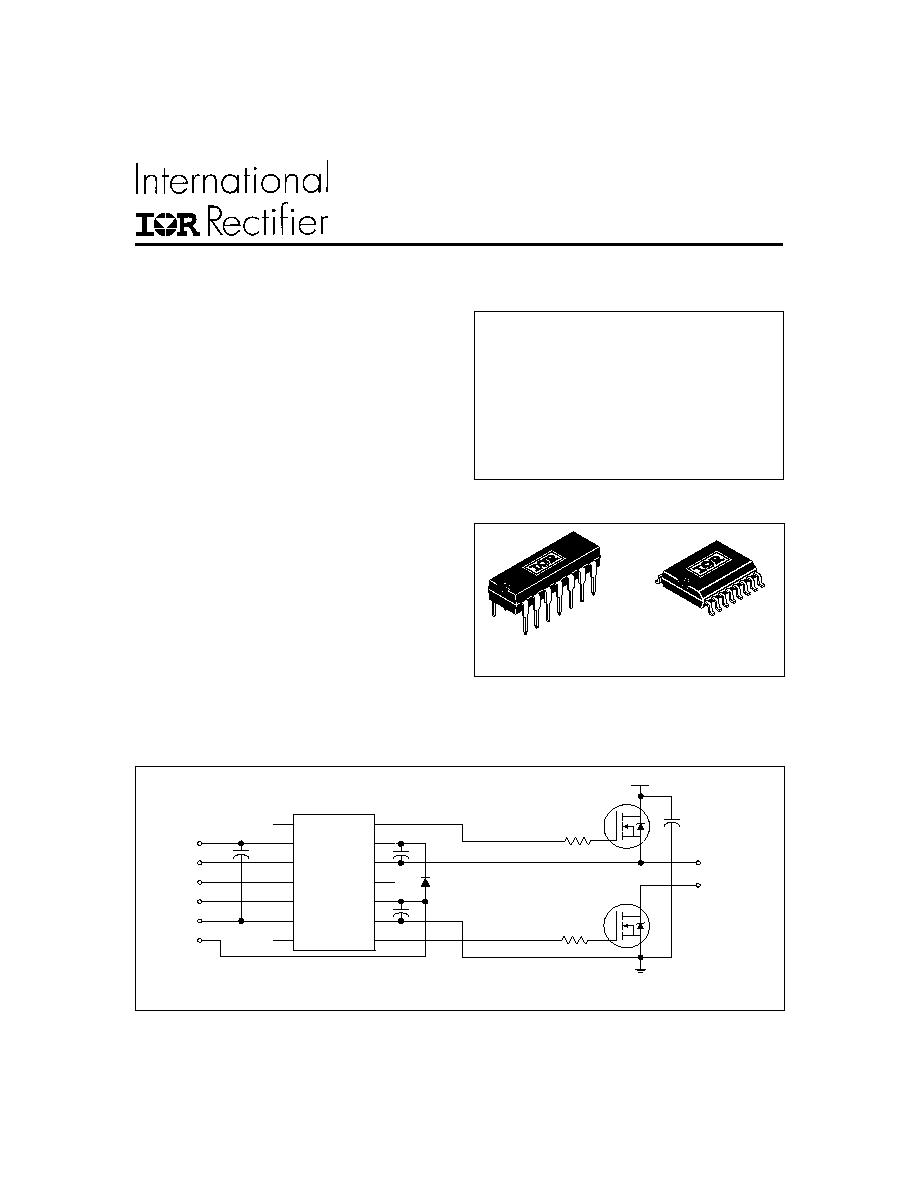
Typical Connection
Features
·
Floating channel designed for bootstrap operation
Fully operational to +1200V
Tolerant to negative transient voltage
dV/dt immune
·
Gate drive supply range from 12 to 20V
·
Undervoltage lockout for both channels
·
3.3V logic compatible
Separate logic supply range from 3.3V to 20V
Logic and power ground ±5V offset
·
CMOS Schmitt-triggered inputs with pull-down
·
Cycle by cycle edge-triggered shutdown logic
·
Matched propagation delay for both channels
·
Outputs in phase with inputs
·
Also available LEAD-FREE (PbF)
Description
The IR2213(S) is a high voltage, high speed power
MOSFET and IGBT driver with independent high and
low side referenced output channels. Proprietary
HVIC and latch immune CMOS technologies enable
ruggedized monolithic construction. Logic inputs are
compatible with standard CMOS or LSTTL outputs,
down to 3.3V logic. The output drivers feature a high
Packages
IR2213(S) & (PbF)
HIGH AND LOW SIDE DRIVER
Product Summary
V
OFFSET
1200V max.
I
O
+/-
1.7A / 2A
V
OUT
12 - 20V
t
on/off
(typ.)
280 & 225 ns
Delay Matching
30 ns
16-Lead SOIC
(wide body)
14-Lead PDIP
Preliminary Data Sheet No. PD60030 rev.O
pulse current buffer stage designed for minimum driver cross-conduction. Propagation delays are matched
to simplify use in high frequency applications. The floating channel can be used to drive an N-channel power
MOSFET or IGBT in the high side configuration which operates up to 1200 volts.
HIN
up to 1200V
TO
LOAD
V
DD
V
B
V
S
HO
LO
COM
HIN
LIN
V
SS
SD
V
CC
LIN
V
DD
SD
V
SS
V
CC
www.irf.com
1
(Refer to Lead Assignments for correct pin configuration). This/These diagram(s) show electrical
connections only. Please refer to our Application Notes and DesignTips for proper circuit board layout.
2
www.irf.com
IR2213(
S
) & (PbF)
Symbol
Definition
Min.
Max.
Units
V
B
High Side Floating Supply Voltage
-0.3
1225
V
S
High Side Floating Supply Offset Voltage
V
B
- 25
V
B
+ 0.3
V
HO
High Side Floating Output Voltage
V
S
- 0.3
V
B
+ 0.3
V
CC
Low Side Fixed Supply Voltage
-0.3
25
V
LO
Low Side Output Voltage
-0.3
V
CC
+ 0.3
V
DD
Logic Supply Voltage
-0.3
V
SS
+ 25
V
SS
Logic Supply Offset Voltage
V
CC
- 25
V
CC
+ 0.3
V
IN
Logic Input Voltage (HIN, LIN & SD)
V
SS
- 0.3
V
DD
+ 0.3
dVs/dt
Allowable Offset Supply Voltage Transient (Figure 2)
--
50
V/ns
P
D
Package Power Dissipation @ T
A
+25°C (14 Lead PDIP)
--
1.6
(16 Lead SOIC)
--
1.25
R
THJA
Thermal Resistance, Junction to Ambient (14 Lead PDIP)
--
75
(16 Lead SOIC)
--
100
T
J
Junction Temperature
--
125
T
S
Storage Temperature
-55
150
T
L
Lead Temperature (Soldering, 10 seconds)
--
300
Symbol
Definition
Min.
Max.
Units
V
B
High Side Floating Supply Absolute Voltage
V
S
+ 12
V
S
+ 20
V
S
High Side Floating Supply Offset Voltage
Note 1
1200
V
HO
High Side Floating Output Voltage
V
S
V
B
V
CC
Low Side Fixed Supply Voltage
12
20
V
LO
Low Side Output Voltage
0
V
CC
V
DD
Logic Supply Voltage
V
SS
+ 3
V
SS
+ 20
V
SS
Logic Supply Offset Voltage
-5 (Note 2)
5
V
IN
Logic Input Voltage (HIN, LIN & SD)
V
SS
V
DD
Absolute Maximum Ratings
Absolute Maximum Ratings indicate sustained limits beyond which damage to the device may occur. All voltage param-
eters are absolute voltages referenced to COM. The Thermal Resistance and Power Dissipation ratings are measured
under board mounted and still air conditions.
Recommended Operating Conditions
The Input/Output logic timing diagram is shown in Figure 1. For proper operation the device should be used within the
recommended conditions. The VS and VSS offset ratings are tested with all supplies biased at 15V differential.
Note 1: Logic operational for V
S
of -5 to +1200V. Logic state held for V
S
of -5V to -V
BS
. (Please refer to the Design Tip
DT97-3 for more details).
Note 2: When V
DD
<5V, the minimum V
SS
offset is limited to -V
DD
°C/W
W
V
V
°C
IR2213(
S
) & (PbF)
www.irf.com
3
Symbol
Definition
Min.
Typ. Max. Units Test Conditions
t
on
Turn-On Propagation Delay
--
280
--
V
S
= 0V
t
off
Turn-Off Propagation Delay
--
225
--
V
S
= 1200V
t
sd
Shutdown Propagation Delay
--
230
--
V
S
= 1200V
t
r
Turn-On Rise Time
--
25
--
t
f
Turn-Off Fall Time
--
17
--
MT
Delay Matching, HS & LS Turn-On/Off
--
--
30
ns
Dynamic Electrical Characteristics
V
BIAS
(V
CC
, V
BS
, V
DD
) = 15V, C
L
= 1000 pF, T
A
= 25
°C and V
SS
= COM unless otherwise specified. The dynamic
electrical characteristics are measured using the test circuit shown in Figure 3.
Symbol
Definition
Min.
Typ. Max. Units Test Conditions
V
IH
Logic "1" Input Voltage
9.5
--
--
V
IL
Logic "0" Input Voltage
--
--
6.0
V
OH
High Level Output Voltage, V
BIAS
- V
O
--
--
1.2
I
O
= 0A
V
OL
Low Level Output Voltage, V
O
--
--
0.1
I
O
= 0A
I
LK
Offset Supply Leakage Current
--
--
50
V
B
= V
S
= 1200V
I
QBS
Quiescent V
BS
Supply Current
--
125
230
V
IN
= 0V or V
DD
I
QCC
Quiescent V
CC
Supply Current
--
180
340
V
IN
= 0V or V
DD
I
QDD
Quiescent V
DD
Supply Current
--
15
30
V
IN
= 0V or V
DD
I
IN+
Logic "1" Input Bias Current
--
20
40
V
IN
= V
DD
I
IN-
Logic "0" Input Bias Current
--
--
1.0
V
IN
= 0V
V
BSUV+
V
BS
Supply Undervoltage Positive Going
8.7
10.2
11.7
Threshold
V
BSUV-
V
BS
Supply Undervoltage Negative Going
7.9
9.3
10.7
Threshold
V
CCUV+
V
CC
Supply Undervoltage Positive Going
8.7
10.2
11.7
Threshold
V
CCUV-
V
CC
Supply Undervoltage Negative Going
7.9
9.3
10.7
Threshold
I
O+
Output High Short Circuit Pulsed Current
1.7
2.0`
--
V
O
= 0V, V
IN
= V
DD
PW
10
µs
I
O-
Output Low Short Circuit Pulsed Current
2.0
2.5
--
V
O
= 15V, V
IN
= 0V
PW
10
µs
µA
V
A
V
Static Electrical Characteristics
V
BIAS
(V
CC
, V
BS
, V
DD
) = 15V, T
A
= 25
°C and V
SS
= COM
unless otherwise specified. The V
IN
, V
TH
and I
IN
parameters
are referenced to V
SS
and are applicable to all three logic input leads: HIN, LIN and SD. The V
O
and I
O
parameters are
referenced to COM and are applicable to the respective output leads: HO or LO.
4
www.irf.com
IR2213(
S
) & (PbF)
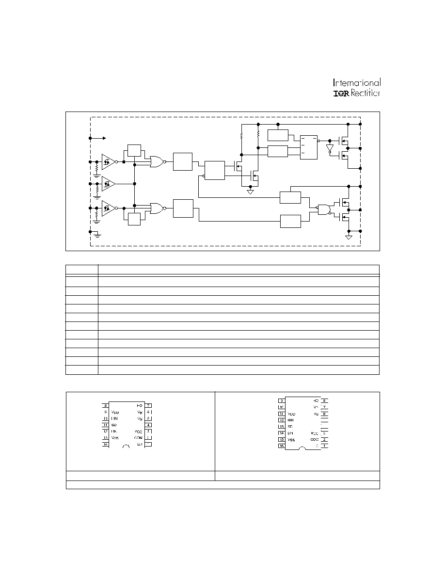
Symbol Description
V
DD
Logic supply
HIN
Logic input for high side gate driver output (HO), in phase
SD
Logic input for shutdown
LIN
Logic input for low side gate driver output (LO), in phase
V
SS
Logic ground
V
B
High side floating supply
HO
High side gate drive output
V
S
High side floating supply return
V
CC
Low side supply
LO
Low side gate drive output
COM
Low side return
Functional Block Diagram
Lead Definitions
Lead Assignments
14 Lead PDIP
16 Lead SOIC (Wide Body)
IR2213
IR2213S
Part Number
V
B
SD
LIN
V
DD
PULSE
GEN
R
S
Q
V
SS
UV
DETECT
DELAY
HV
LEVEL
SHIFT
V
CC
PULSE
FILTER
UV
DETECT
V
DD
/V
CC
LEVEL
SHIFT
V
DD
/V
CC
LEVEL
SHIFT
LO
V
S
COM
R
S
Q
R
S
R
Q
HIN
HO
IR2213(
S
) & (PbF)
www.irf.com
5
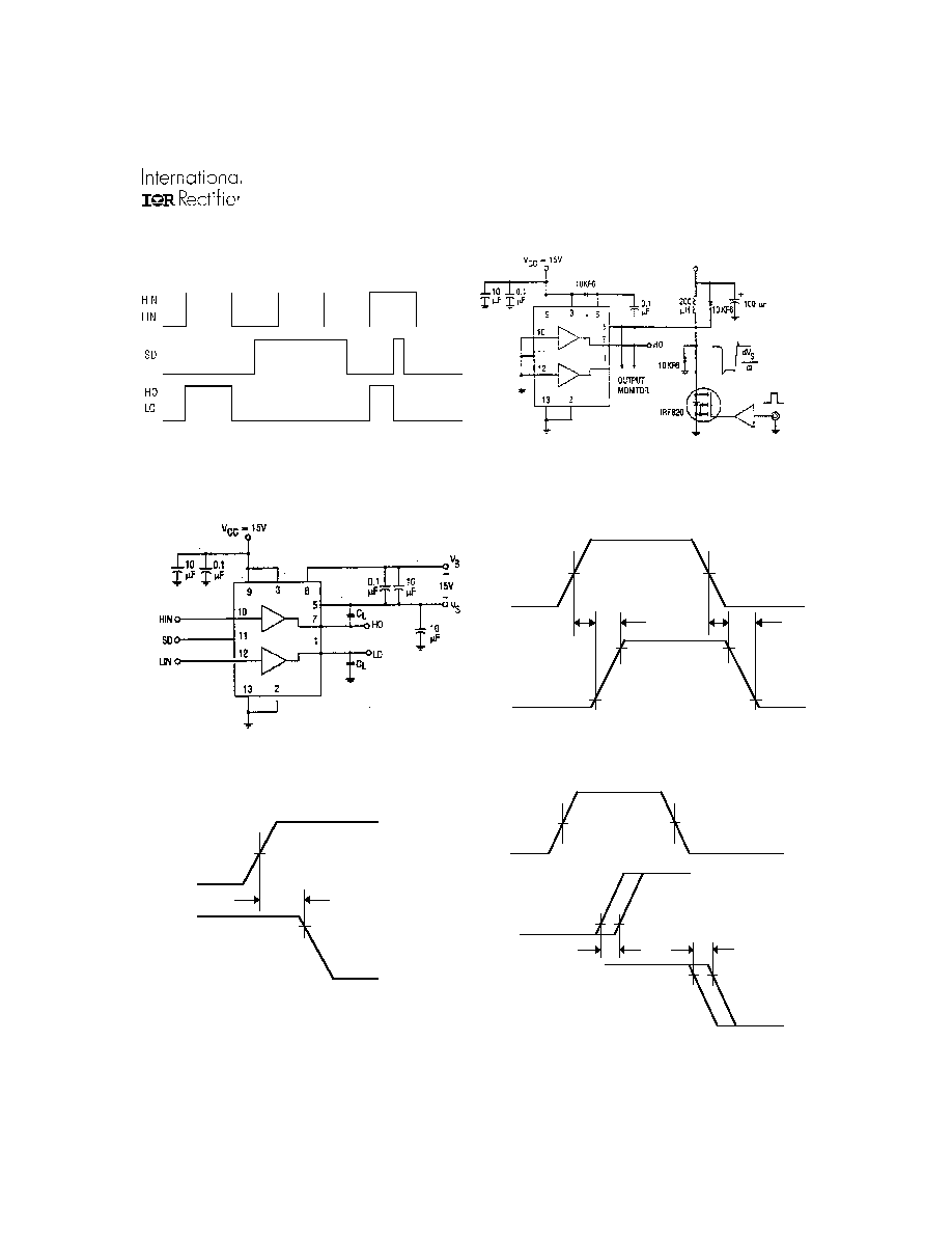
Figure 1. Input/Output Timing Diagram
Figure 2. Floating Supply Voltage Transient Test Circuit
Figure 3. Switching Time Test Circuit
Figure 4. Switching Time Waveform Definition
Figure 6. Delay Matching Waveform Definitions
HIN
LIN
tr
ton
tf
toff
HO
LO
50%
50%
90%
90%
10%
10%
HIN
LIN
HO
50%
50%
10%
LO
90%
MT
HO
LO
MT
(0 to 1200V)
Figure 5. Shutdown Waveform Definitions
SD
tsd
HO
LO
50%
90%
HV =10 to 1200V
<50 V/ns