
Typical Application
Product Summary
V
OFFSET
600Vmax
I
QBS
1mA
Overcurrent trip
1.5usec (typ)
signal delay
Overcurrent trip level +/-260mV (typ.)
OVER CURRENT SENSING IC
Features
·
Floating channel up to +600V
·
Monolithic integration
·
Overcurrent sensing through shunt resistor
·
Low I
QBS
allows the boot strap power supply
·
Independent fast 1
µ
sec overcurrent trip signal
·
High common mode noise immunity
·
Input overvoltage protection for IGBT short circuit
condition
·
Open Drain outputs
Description
IR2170(S) is the monolithic over current sensing IC de-
signed for motor drive applications. It senses the motor
phase current through an external shunt resistor, de-
tects overcurrent condition, and transfers the signal to
the low side. IR's proprietary high voltage isolation tech-
nology is implemented to enable the high bandwidth sig-
nal processing. The dedicated overcurrent trip (OC)
signal facilitates IGBT short circuit protection. The OC
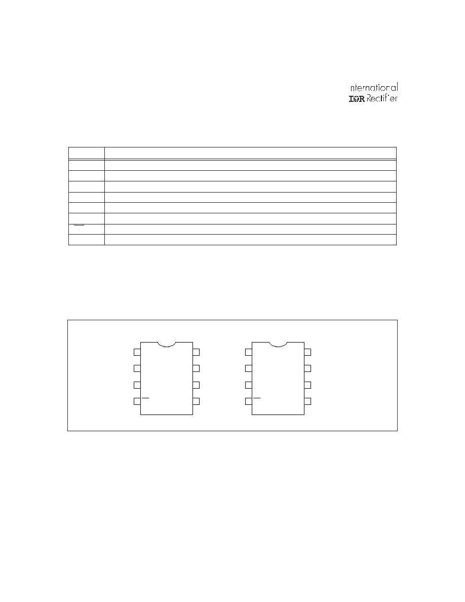
Packages
8-Lead SOIC
IR2170
(
S
)
(Refer to Lead Assignments for correct pin configuration). This/These diagram(s) show electrical connections only. Please
refer to our Application Notes and DesignTips for proper circuit board layout.
8-Lead PDIP
Preliminary Data Sheet No. PD60186-C
DC Bus (up to 600V)
To Motor Phase
R
SENSE
+15V
+
(AGND)
Vdd
(DGND)
V
IN+
V
IN-
V
B
V
S
V
CC
COM
OC
(Circuit Common = DC Bus Negative)
10 uF
0.47 uF
10 nF
1 k
(typ)
1
IR2170
output pulse width can be programmed by the external resistor and capacitor. The open-drain outputs make easy for
any interface from 3.3V to 15V.

2
IR2170
(
S
)
www.irf.com
Symbol Definition
Min.
Max.
Units
V
S
High side offset voltage
-0.3
600
V
BS
High side floating supply voltage
-0.3
25
V
CC
Low side and logic fixed supply voltage
-0.3
25
V
IN
Maximum input voltage between V
IN+ and
V
IN-
-5
5
V
OC
Overcurrent output voltage
COM -0.3
VCC +0.3
V
IN-
V
IN-
input voltage (note 1)
V
S
-5
V
B+
0.3
dV/dt
Allowable offset voltage slew rate
--
50
V/ns
P
D
Package power dissipation @ T
A
+25
°C
8 lead SOIC
--
.625
8 lead PDIP
--
1.0
Rth
JA
Thermal resistance, junction to ambient
8 lead SOIC
--
200
8 lead PDIP
--
125
T
J
Junction temperature
--
150
T
S
Storage temperature
-55
150
T
L
Lead temperature (soldering, 10 seconds)
--
300
Absolute Maximum Ratings
Absolute maximum ratings indicate sustained limits beyond which damage to the device may occur. All voltage
parameters are absolute voltages referenced to COM, all currents are defined positive into any lead. The thermal
resistance and power dissipation ratings are measured under board mounted and still air conditions.
V
°C/W
W
Note 1: Capacitors are required between V
B
and Vin-, and between V
B
and Vs pins when bootstrap power
is used. The external power supply, when used, is required between Vs and Vin-, and between V
B
and Vs
pins.
°C
Recommended Operating Conditions
The output logic timing diagram is shown in figure 1. For proper operation the device should be used within the recom-
mended conditions.
Symbol Definition
Min.
Max.
Units
V
B
High side floating supply voltage
V
S
+13.0
V
S
+20
V
S
High side floating supply offset voltage
note 2
600
V
OC
Overcurrent output voltage
COM
VCC
V
CC
Low side and logic fixed supply voltage
9.5
20
V
IN
Input voltage between V
IN+
and V
IN-
-260
+260
mV
T
A
Ambient temperature
-40
125
°C
V
Note 2: Logic operation for Vs of -5 to +600V. Logic state held for Vs of -5V to -V
BS
.
(Please refer to the Design
Tip DT97-3 for more details).

3
IR2170
(
S
)
www.irf.com
V
OC+
Overcurrent trip positive input voltage
--
260
--
V
OC-
Overcurrent trip negative input voltage
--
-260
--
I
LK
Offset supply leakage current
--
--
50
µA
V
B
= V
S
= 600V
I
QBS
Quiescent V
BS
supply current
--
1
2
V
S
= 0V
I
QCC
Quiescent V
CC
supply current
--
--
0.5
I
OCC
OC output sink current
10
--
--
1
--
--
DC Electrical Characteristics
V
CC
= V
BS
= 15V, and T
A
= 25
o
C unless otherwise specified.
Symbol
Definition
Min. Typ. Max. Units Test Conditions
V
O
= 1V
V
O
= 0.1V
mA
mV
AC Electrical Characteristics
V
CC
= V
BS
= 15V, and T
A
= 25
o
C unless otherwise specified.
Symbol
Definition
Min. Typ. Max. Units Test Conditions
Proagation delay characteristics
tdoc
Propagation delay time of OC
1
1.5
--
twoc
Low true pulse width of OC
--
1
--
µ
sec
Figure 1. OC Waveform
+260mV
-260mV
Vin
OC
t
woc
t
doc
4
IR2170
(
S
)
www.irf.com
IR2170S
8
7
6
4
3
2
1
VCC
OC
NC
COM
VS
VIN-
VIN+
VB
5
8 lead SOIC
IR2170
8
7
6
4
3
2
1
VCC
OC
NC
COM
VS
VIN-
VIN+
VB
5
8 lead PDIP
Lead Definitions
Symbol Description
V
CC
Low side and logic supply voltage
COM
Low side logic ground
V
IN+
Positive sense input
V
IN-
Negative sense input
V
B
High side supply
V
S
High side return
OC
Overcurrent output (negative logic)
N.C.
No connection
Lead Assignments

5
IR2170
(
S
)
www.irf.com
01-6014
01-3003 01
(MS-001AB)
8-Lead PDIP
Case outlines
01-6027
01-0021 11
(MS-012AA)
8-Lead SOIC
8
7
5
6
5
D
B
E
A
e
6X
H
0.25 [.010]
A
6
4
3
1
2
4. OUTLINE CONFORMS TO JEDEC OUTLINE MS-012AA.
NOTES:
1. DIMENSIONING & TOLERANCING PER ASME Y14.5M-1994.
2. CONTROLLING DIMENSION: MILLIMETER
3. DIMENSIONS ARE SHOWN IN MILLIMETERS [INCHES].
7
K x 45°
8X L
8X c
y
FOOTPRINT
8X 0.72 [.028]
6.46 [.255]
3X 1.27 [.050]
8X 1.78 [.070]
5 DIMENSION DOES NOT INCLUDE MOLD PROTRUSIONS.
6 DIMENSION DOES NOT INCLUDE MOLD PROTRUSIONS.
MOLD PROTRUSIONS NOT TO EXCEED 0.25 [.010].
7 DIMENSION IS THE LENGTH OF LEAD FOR SOLDERING TO
A SUBSTRATE.
MOLD PROTRUSIONS NOT TO EXCEED 0.15 [.006].
0.25 [.010]
C A B
e1
A
A1
8X b
C
0.10 [.004]
e 1
D
E
y
b
A
A1
H
K
L
.189
.1497
0°
.013
.050 BASIC
.0532
.0040
.2284
.0099
.016
.1968
.1574
8°
.020
.0688
.0098
.2440
.0196
.050
4.80
3.80
0.33
1.35
0.10
5.80
0.25
0.40
0°
1.27 BASIC
5.00
4.00
0.51
1.75
0.25
6.20
0.50
1.27
MIN
MAX
MILLIMETERS
INCHES
MIN
MAX
DIM
8°
e
c
.0075
.0098
0.19
0.25
.025 BASIC
0.635 BASIC
10/24/2002