Äîêóìåíòàöèÿ è îïèñàíèÿ www.docs.chipfind.ru
Features
·
Ballast control and half-bridge driver in one IC
·
Programmable preheat frequency
·
Programmable preheat time
·
Internal ignition ramp
·
Programmable over-current threshold
·
Programmable run frequency
Data Sheet No. PD60182-I
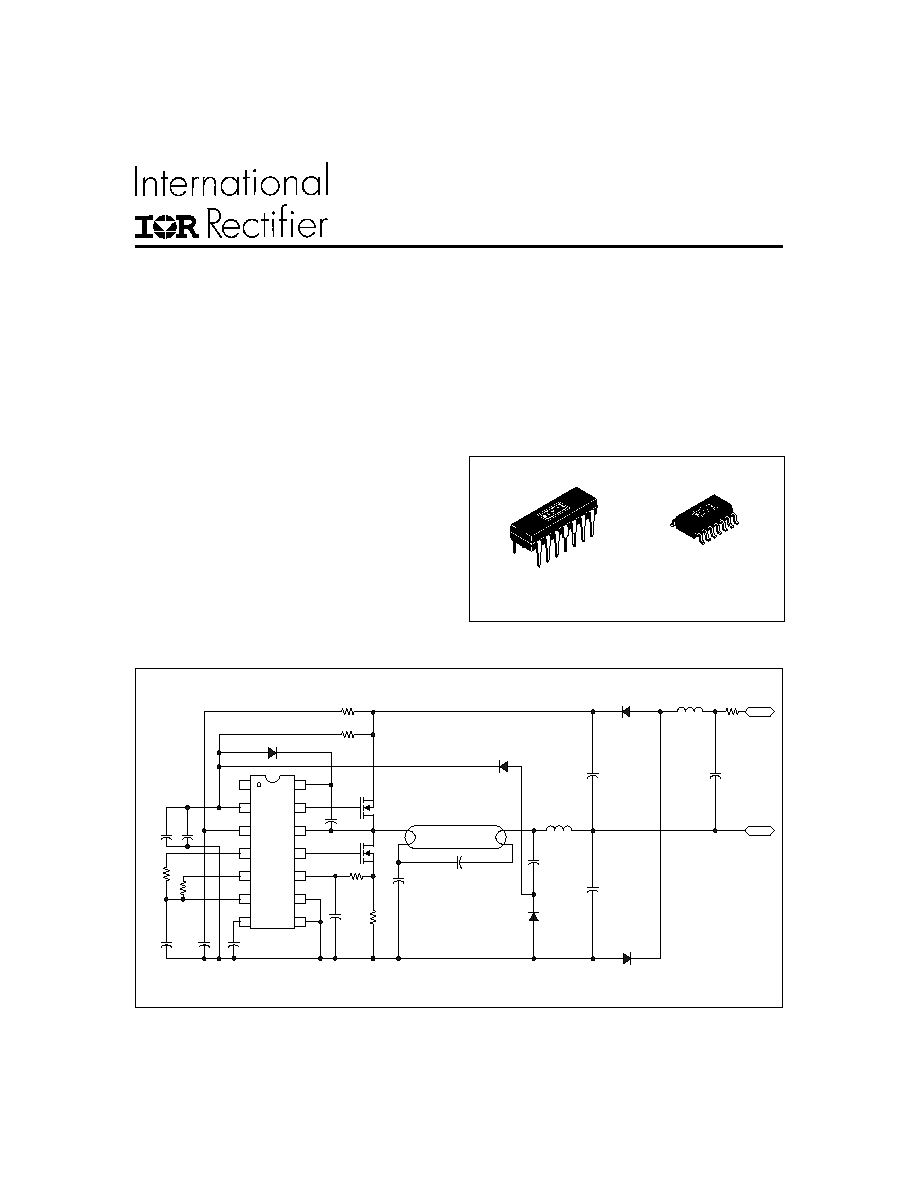
BALLAST CONTROL IC
CFL Application Diagram
·
Programmable dead time
·
DC bus under-voltage reset
·
Shutdown pin with hysteresis
·
Internal 15.6V zener clamp diode on Vcc
·
Micropower startup (150
µ
A)
·
Latch immunity and ESD protection
·
Also available LEAD-FREE (PbF)
Description
The IR2156 incorporates a high voltage half-bridge
gate driver with a programmable oscillator and state
diagram to form a complete ballast control IC. The
IR2156 features include programmable preheat and
run frequencies, programmable preheat time, program-
mable dead-time, and programmable over-current pro-
tection. Comprehensive protection features such as
protection from failure of a lamp to strike,filament fail-
ures, as well as an automatic restart function, have
been included in the design. The IR2156 is available in
both 14 lead PDIP and 14 lead SOIC packages.
www.irf.com
1
Packages
14 Lead PDIP
14 Lead SOIC
(narrow body)
L
RES
C
VCC1
M2
M1
1
2
3
4
5
6
7
14
13
12
11
10
9
8
IR2156
RT
RPH
VDC
CPH
CS
LO
VS
HO
VB
COM
C
BOOT
CT
SD
C
RES
L
N
NC
F1
L
FILTE
R
C
FILTE
R
R
PH
R
T
C
CPH
C
T
R
1
C
SNUB
C
CP
D
CP1
D
CP2
C
ELCAP1
C
ELCAP1
D
RECT1
D
RECT2
VCC
C
VCC2
C
VDC
D
BOOT
R
BUS
R
SUPPLY
R
CS
C
CS
IR2156
(S) & (PbF)
IR2156
(S) & (PbF)
2
www.irf.com
Absolute Maximum Ratings
Absolute maximum ratings indicate sustained limits beyond which damage to the device may occur. All voltage
parameters are absolute voltages referenced to COM, all currents are defined positive into any lead. The thermal
resistance and power dissipation ratings are measured under board mounted and still air conditions.
Note 1:
This IC contains a zener clamp structure between the chip V
CC
and COM which has a nominal breakdown
voltage of 15.6V. Please note that this supply pin should not be driven by a DC, low impedance power source
greater than the V
CLAMP
specified in the Electrical Characteristics section.
Symbol Definition
Min.
Max.
Units
V
B
High side floating supply voltage
-0.3
625
V
S
High side floating supply offset voltage
V
B
- 25
V
B
+ 0.3
V
HO
High side floating output voltage
V
S
- 0.3
V
B
+ 0.3
V
LO
Low side output voltage
-0.3
V
CC
+ 0.3
I
OMAX
Maximum allowable output current (HO, LO)
-500
500
due to external power transistor miller effect
V
VDC
VDC pin voltage
-0.3
V
CC
+ 0.3
V
CT
CT pin voltage
-0.3
V
CC
+ 0.3
V
CC
+ 0.3
I
CPH
CPH pin current
-5
5
I
RPH
RPH pin current
-5
5
V
RPH
RPH pin voltage
-0.3
V
CC
+ 0.3
V
I
RT
RT pin current
-5
5
mA
V
RT
RT pin voltage
-0.3
V
CC
+ 0.3
V
CS
Current sense pin voltage
-0.3
5.5
I
CS
Current sense pin current
-5
5
I
SD
Shutdown pin current
-5
5
I
CC
Supply current (note 1)
-20
20
dV/dt
Allowable offset voltage slew rate
-50
50
V/ns
P
D
Package power dissipation @ T
A
+25
°C
(14 pin PDIP)
--
1.70
P
D =
(T
JMAX
-T
A
)/Rth
JA
(14 pin SOIC)
--
1.00
Rth
JA
Thermal resistance, junction to ambient
(14 pin PDIP)
--
70
(14 pin SOIC)
--
120
T
J
Junction temperature
-55
150
T
S
Storage temperature
-55
150
T
L
Lead temperature (soldering, 10 seconds)
--
300
V
mA
mA
V
mA
V
W
o
C/W
o
C
IR2156
(S) & (PbF)
www.irf.com
3
Recommended Operating Conditions
For proper operation the device should be used within the recommended conditions.
Symbol Definition
Min.
Max.
Units
V
B
s
High side floating supply voltage
V
CC
- 0.7
V
CLAMP
V
BSMIN
Minimum required VBS voltage for proper HO functionality
5
V
CC
V
S
Steady state high side floating supply offset voltage
-1
600
V
CC
Supply voltage
V
CCUV+
V
CLAMP
I
CC
Supply current
note 2
10
mA
C
T
CT lead capacitance
220
--
pF
I
SD
Shutdown lead current
-1
1
I
CS
Current sense lead current
-1
1
T
J
Junction temperature
-40
125
o
C
I
SDLK
SD pin leakage current (@V
SD
=6V)
--
125
I
CSLK
CS pin leakage current (@V
CS
=3V)
--
25
V
mA
Note 2:
Enough current should be supplied into the V
CC
lead to keep the internal 15.6V zener clamp diode on this lead
regulating its voltage, V
CLAMP
.
Electrical Characteristics
V
CC
= V
BS
= V
BIAS
= 14V +/- 0.25V, V
VDC
= Open, R
T
= 39.0k
, R
PH
= 100.0k
,
C
T
= 470 pF, V
CPH
= 0.0V, V
CS
= 0.0V,
V
SD
= 0.0V, C
LO, HO
= 1000pF, T
A
= 25
o
C unless otherwise specified.
Symbol Definition
Min.
Typ.
Max. Units Test Conditions
Supply Characteristics
V
CCUV+
V
CC
supply undervoltage positive going
10.5
11.5
12.5
V
CC
rising from 0V
threshold
V
CCUV-
V
CC
supply undervoltage negative going 8.5 9.5
10.5
V
CC
falling from 14V
threshold
V
UVHYS
V
CC
supply undervoltage lockout hysteresis
1.5 2.0
3.0
I
QCCUV
UVLO mode quiescent current
50 120
200
V
CC
= 11V
I
QCCFLT
Fault-mode quiescent current
-- 200
470
SD = 5.1V, or
CS > 1.3V
I
QCC
Quiescent V
CC
supply current
-- 1.0
1.5
CT
connected to
COM
VCC =14V,RT=15k
I
QCC50K
V
CC
supply current, f = 50kHz
-- 1.0
1.5
RT = 15k
C
T
= 470 pF
V
CLAMP
V
CC
zener clamp voltage
14.5 15.6 16.5
V
I
CC
= 5mA
µ
A
V
mA
I
QBS0
Quiescent V
BS
supply current
-5
0
5
V
HO
= V
S
(C
T
= 0V)
I
QBS1
Quiescent V
BS
supply current
--
30
50
V
HO
= V
B
(C
T
= 14V)
I
LK
Offset supply leakage current
--
--
50
µ
A
V
B
= V
S
= 600V
µ
A
Floating Supply Characteristics
µ
A
IR2156
(S) & (PbF)
4
www.irf.com
Electrical Characteristics
V
CC
= V
BS
= V
BIAS
= 14V +/- 0.25V, V
VDC
= Open, R
T
= 39.0k
, R
PH
= 100.0k
,
C
T
= 470 pF, V
CPH
= 0.0V, V
CS
= 0.0V,
V
SD
= 0.0V, C
LO, HO
= 1000pF, T
A
= 25
o
C unless otherwise specified.
Symbol Definition
Min.
Typ.
Max. Units Test Conditions
RPH Characteristics
I
RPHLK
Open circuit RPH pin leakage current
--
0.1
--
µ
A CT = 10V
V
RPHFLT
Fault-mode RPH pin voltage
--
0
--
mV SD
> 5.1V
or CS >1.3V
Oscillator, Ballast Control, I/O Characteristics
kHz
fosc Oscillator frequency
28
30
32
R
T
=33.0k
, V
VDC
= 5V
V
CPH
= Open
(Guaranteed by design)
fosc
Oscillator frequency
37.6
40
43.9
KHz
R
T
=40k, R
PH
= 100K
C
T
= 470pF
d
Oscillator duty cycle
--
50
--
%
V
CT+
Upper C
T
ramp voltage threshold
--
8.3
--
V
CT-
Lower C
T
ramp voltage threshold
--
4.8
--
V
CTFLT
Fault-mode C
T
pin voltage
--
0
-- mV SD
> 5.1V
or CS >1.3V
only CT CAP should
beconnected to CT
t
DLO
LO output deadtime
--
2.0
--
usec
t
DHO
HO output deadtime
--
2.0
--
usec
R
DT
Internal deadtime resistor
--
3
--
K
V V
CC
= 14V
RT Characteristics
I
RTLK
Open circuit RT pin leakage current
--
0.1
--
µ
A CT = 10V
V
RTFLT
Fault-mode RT pin voltage
--
0
--
mV SD
> 5.1V
or CS >1.3V
Preheat Characteristics
I
CPH
CPH pin charging current
3.6
4.3 5.2
µ
A
VCPH=10V,CT=10V,
VDC=5V
V
CPHFLT
Fault-mode CPH pin voltage
--
0
--
mV SD
> 5.1V
or CS >1.3V
V
SDTH+
Rising shutdown pin threshold voltage
--
5.1
--
V
V
SDHYS
Shutdown pin threshold hysteresis
-- 450
--
mV
V
CSTH
Over-current sense threshold voltage
1.1 1.25
1.44
V
t
CS
Over-current sense propogation delay
-- 160
--
nsec Delay from CS to LO
V
CSPW
Over-current sense minimum pulse width
--
135
--
nsec V
CS
pulse amplitude
= V
CSTH
+100mV
R
VDC
DC bus sensing resistor
7.5 10
14
k
V
CPH
>12V, VCT=0V
VDC= 7V
V
CPH-VDC
CPH to VDC offset voltage
10.3 10.9
11.4
V V
CPH
=open,V
VDC=
0V
Protection Characteristics
V
OL
Low-level output voltage
--
0
105
Io = 0
V
OH
High-level output voltage
--
0
100
V
BIAS
- Vo, Io = 0
tr
Turn-on rise time
--
110
150
tf
Turn-off fall time
--
55
100
Gate Driver Output Characteristics
mV
ns
C
LO
= C
HO
=1nF
IR2156
(S) & (PbF)
www.irf.com
5
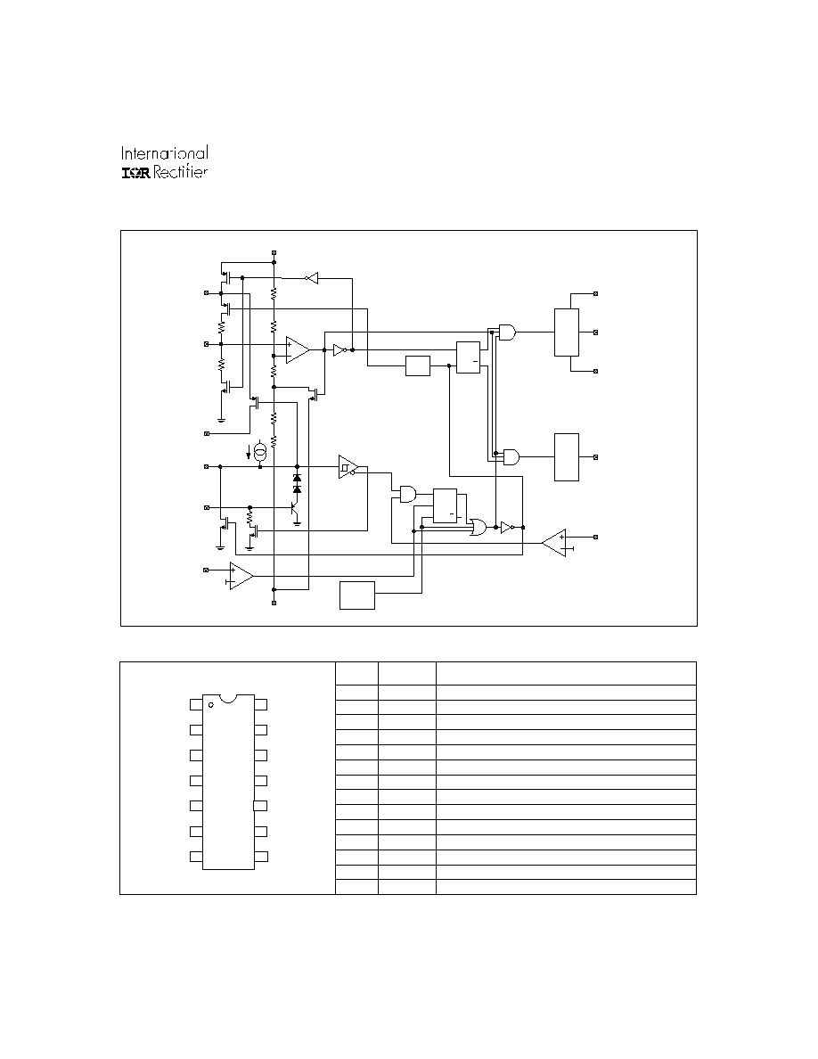
Lead Assignments & Definitions
Block Diagram
Pin Assignments
1
2
3
4
5
6
7
10
9
8
IR2156
NC
VCC
VDC
RT
RPH
COM
CT
CS
LO
VS
HO
VB
CPH
SD
14
13
12
11
Pin # Symbol
Description
1
14
13
3
12
7
6
5
4
2
RT
VS
HO
NC
SD
CPH
CT
RPH
Minimum frequency timing resistor
Preheat frequency timing resistor
Oscillator timing capacitor
Preheat timing capacitor
High-side gate driver output
High-side floating return
CS
Current sensing input
9
11
10
8
LO
VB
VCC
COM
IC power & signal ground
Logic & low-side gate driver supply
High-side gate driver floating supply
Low-side gate driver output
Shutdown input
No connect
VDC
IC start-up and DC bus sensing Input
RT
CPH
VB
HO
VS
LO
CS
Vcc
CT
RPH
COM
R
V
TH
R
ICPH
R
Under-
Voltage
Detect
Fault
Logic
Driver
Logic
High-
Side
Driver
Low-
Side
Driver
Comp 1
Schmitt 1
SD
5.1V
Soft
Start
1.3V
R
R
2.5K
40K
S1
S2
S3
S4
Q
T
R
Q
S6
Comp 2
Comp 3
Q
S
R2 Q
R1
VDC
10K
5.1V
5.1V
RDT
RVDC