Äîêóìåíòàöèÿ è îïèñàíèÿ www.docs.chipfind.ru
Features
·
Integrated 600V half-bridge gate driver
·
15.6V zener clamp on Vcc
·
True micropower start up
·
Tighter initial deadtime control
·
Low temperature coefficient deadtime
·
Shutdown feature (1/6th Vcc) on C
T
pin
·
Increased undervoltage lockout Hysteresis (1V)
·
Lower power level-shifting circuit
·
Constant LO, HO pulse widths at startup
·
Lower di/dt gate driver for better noise immunity
·
Low side output in phase with R
T
·
Internal 50nsec (typ.) bootstrap diode (IR21531D)
·
Excellent latch immunity on all inputs and outputs
·
ESD protection on all leads
·
Also available LEAD_FREE
Preliminary Data Sheet No. PD60131-L
SELF-OSCILLATING HALF-BRIDGE DRIVER
Product Summary
V
OFFSET
600V max.
Duty Cycle
50%
Tr/Tp
80/40ns
V
clamp
15.6V
Deadtime (typ.)
0.6
µs
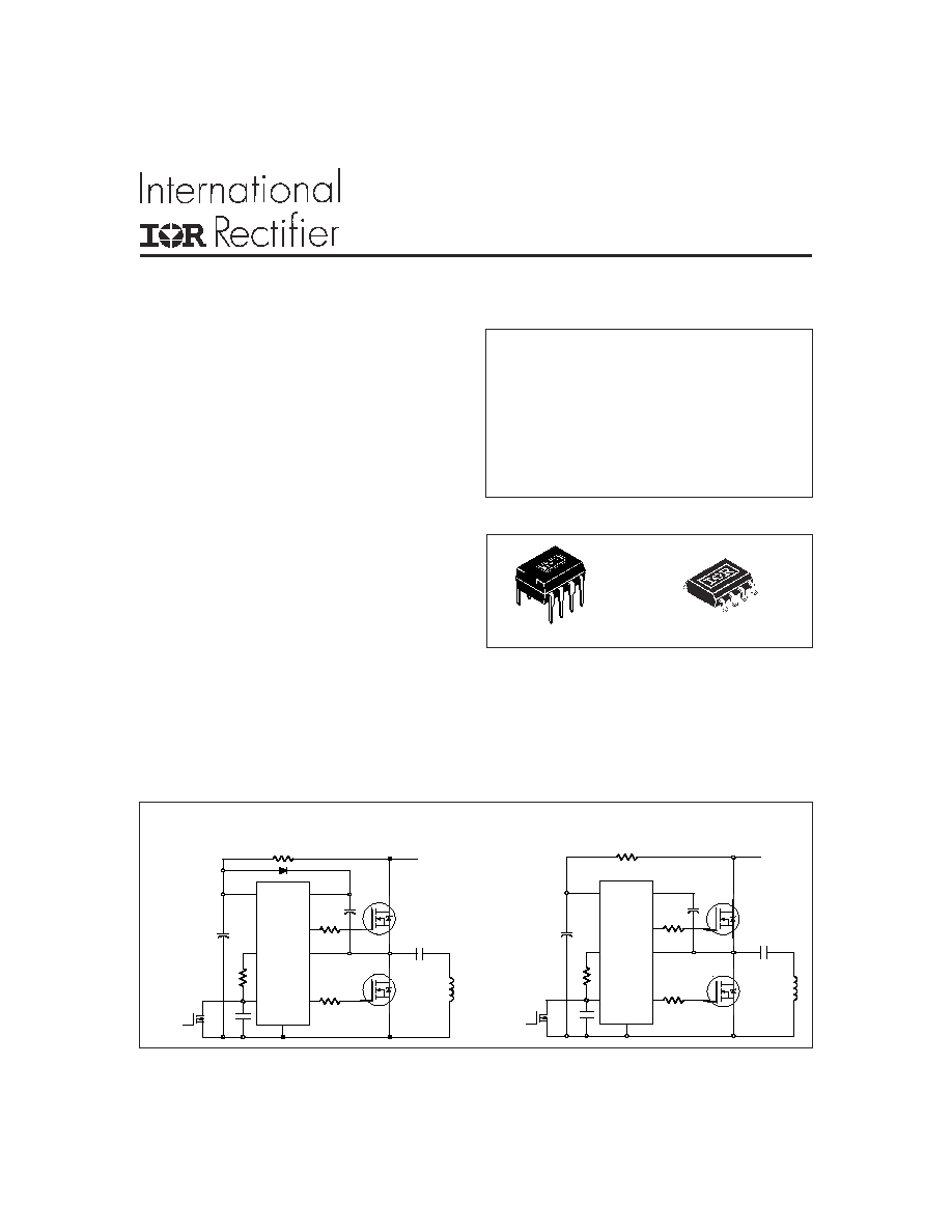
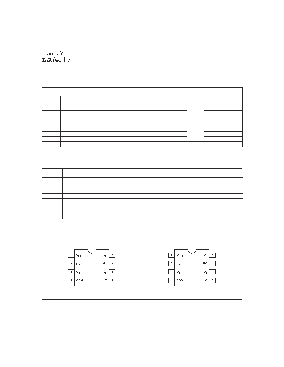
Typical Connections
IR21531D(S) & (PbF)
Description
The IR21531(D)(S) are an improved version of the
popular IR2155 and IR2151 gate driver ICs, and in-
corporates a high voltage half-bridge gate driver with a front end oscillator similar to the industry standard
CMOS 555 timer. The IR21531 provides more functionality and is easier to use than previous ICs. A shutdown
feature has been designed into the CT pin, so that both gate driver outputs can be disabled using a low voltage
control signal. In addition, the gate driver output pulse widths are the same once the rising undervoltage
lockout threshold on VCC has been reached, resulting in a more stable profile of frequency vs time at
startup. Noise immunity has been improved significantly, both by lowering the peak di/dt of the gate drivers,
and by increasing the undervoltage lockout hysteresis to 1V. Finally, special attention has been payed to
maximizing the latch immunity of the device, and providing comprehensive ESD protection on all pins.
IR21531D
IR21531(S)
VB
HO
VS
LO
VCC
RT
CT
COM
600V
MAX
Shutdown
VB
HO
VS
LO
VCC
RT
CT
COM
600V
MAX
Shutdown
www.irf.com
1
Packages
8 Lead PDIP
8 Lead SOIC
IR21531D(S) & (PbF)
2
www.irf.com
Note 1:
This IC contains a zener clamp structure between the chip V
CC
and COM which has a nominal breakdown
voltage of 15.6V. Please note that this supply pin should not be driven by a DC, low impedance power source
greater than the V
CLAMP
specified in the Electrical Characteristics section.
Note 2:
Care should be taken to avoid output switching conditions where the V
S
node flies inductively below ground by
more than 5V.
Note 3:
Enough current should be supplied to the V
CC
pin of the IC to keep the internal 15.6V zener diode clamping the
voltage at this pin.
Recommended Operating Conditions
For proper operation the device should be used within the recommended conditions.
Symbol Definition
Min.
Max.
Units
V
BS
High side floating supply voltage
V
CC
- 0.7
V
CLAMP
V
S
Steady state high side floating supply offset voltage
-3.0 (note 2)
600
V
CC
Supply voltage
10
V
CLAMP
I
CC
Supply current
(note 3)
5
mA
T
J
Junction temperature
-40
125
°C
V
Absolute Maximum Ratings
Absolute maximum ratings indicate sustained limits beyond which damage to the device may occur. All voltage param-
eters are absolute voltages referenced to COM, all currents are defined positive into any lead. The thermal resistance and
power dissipation ratings are measured under board mounted and still air conditions.
Symbol Definition
Min.
Max.
Units
V
B
High side floating supply voltage
-0.3
625
V
S
High side floating supply offset voltage
V
B
- 25
V
B
+ 0.3
V
HO
High side floating output voltage
V
S
- 0.3
V
B
+ 0.3
V
LO
Low side output voltage
-0.3
V
CC
+ 0.3
V
RT
R
T
pin voltage
-0.3
V
CC
+ 0.3
V
CT
C
T
pin voltage
-0.3
V
CC
+ 0.3
I
CC
Supply current (note 1)
--
25
I
RT
R
T
pin current
-5
5
dV
s
/dt
Allowable offset voltage slew rate
-50
50
V/ns
P
D
Maximum power dissipation @ T
A
+25
°C
(8 Lead DIP)
--
1.0
(8 Lead SOIC)
--
0.625
Rth
JA
Thermal resistance, junction to ambient
(8 Lead DIP)
--
125
(8 Lead SOIC)
--
200
T
J
Junction temperature
-55
150
T
S
Storage temperature
-55
150
°C
T
L
Lead temperature (soldering, 10 seconds)
--
300
V
°C/W
W
mA
IR21531D(S) & (PbF)
www.irf.com
3
Symbol Component
Min.
Max.
Units
R
T
Timing resistor value
10
--
k
C
T
C
T
pin capacitor value
330
--
pF
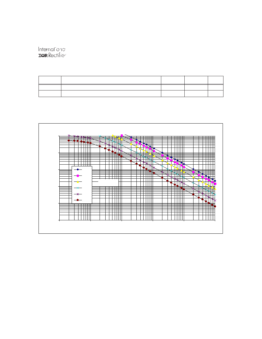
Recommended Component Values
IR2153 RT vs Frequency
10
100
1000
10000
100000
1000000
10
100
1000
10000
100000
1000000
RT (ohms)
Frequency (Hz)
330pf
470pF
1nF
2.2nF
4.7nF
10nF
CT Values
IR21531 RT vs Frequency
IR21531D(S) & (PbF)
4
www.irf.com
Floating Supply Characteristics
Electrical Characteristics
V
BIAS
(V
CC
, V
BS
) = 12V, C
L
= 1000 pF, C
T
= 1 nF and T
A
= 25
°C unless otherwise specified. The V
IN
, V
TH
and I
IN
parameters are referenced to COM. The V
O
and I
O
parameters are referenced to COM and are applicable to the
respective output leads: HO or LO.
Symbol Definition
Min. Typ. Max. Units Test Conditions
V
CCUV+
Rising V
CC
undervoltage lockout threshold
8.1
9.0 9.9
V
CCUV-
Falling V
CC
undervoltage lockout threshold
7.2
8.0 8.8
V
CCUVH
V
CC
undervoltage lockout Hysteresis
0.5
1.0
1.5
I
QCCUV
Micropower startup V
CC
supply current
--
75
150
V
CC
V
CCUV
-
I
QCC
Quiescent V
CC
supply current
--
500 950
V
CLAMP
V
CC
zener clamp voltage
14.4
15.6 16.8
V
I
CC
= 5mA
Low Voltage Supply Characteristics
V
µ
A
Symbol Definition
Min.
Typ.
Max. Units Test Conditions
fosc
Oscillator frequency
19.4
20
20.6
R
T
= 36.9k
94
100
106
R
T
= 7.43k
d R
T
pin duty cycle
48
50
52
%
fo < 100kHz
I
CT
C
T
pin current
--
0.001
1.0
uA
I
CTUV
UV-mode C
T
pin pulldown current
0.30
0.70
1.2
mA
V
CC
= 7V
V
CT+
Upper C
T
ramp voltage threshold
--
8.0
--
V
CT-
Lower C
T
ramp voltage threshold
--
4.0
--
V
CTSD
C
T
voltage shutdown threshold
1.8
2.1
2.4
V
RT+
High-level R
T
output voltage, V
CC
- V
RT
--
10
50
I
RT
= 100
µ
A
--
100
300
I
RT
= 1mA
V
RT-
Low-level R
T
output voltage
--
10
50
I
RT
= 100
µ
A
--
100
300
I
RT
= 1mA
V
RTUV
UV-mode R
T
output voltage
--
0
100
V
CC
V
CCUV
-
V
RTSD
SD-Mode R
T
output voltage, V
CC
- V
RT
--
10
50
I
RT
= 100
µ
A,
V
CT
= 0V
--
10
300
I
RT
= 1mA,
V
CT
= 0V
Oscillator I/O Characteristics
V
mV
Symbol Definition
Min.
Typ.
Max. Units Test Conditions
I
QBSUV
Micropower startup V
BS
supply current
--
0
10
V
CC
V
CCUV
-
I
QBS
Quiescent VBS supply current
-- 30
50
V
BSMIN
Minimum required V
BS
voltage for proper
-- 4.0 5.0
V V
CC
=V
CCUV+
+ 0.1V
functionality from R
T
to HO
I
LK
Offset supply leakage current
--
--
50
µ
A
V
B
= V
S
= 600V
V
F
Bootstrap diode forward voltage (IR21531D)
0.5
--
1.0
V
I
F
= 250mA
µ
A
kHz
IR21531D(S) & (PbF)
www.irf.com
5
Lead Assignments
8 Lead DIP
8 Lead SOIC
IR21531(D)
IR21531S
NOTE: The IR21531D is offered in 8 lead DIP only.
Symbol
Description
V
CC
Logic and internal gate drive supply voltage
R
T
Oscillator timing resistor input
C
T
Oscillator timing capacitor input
COM
IC power and signal ground
LO
Low side gate driver output
V
S
High voltage floating supply return
HO
High side gate driver output
V
B
High side gate driver floating supply
Lead Definitions
Symbol Definition
Min.
Typ.
Max. Units Test Conditions
V
OH
High level output voltage, V
BIAS
-V
O
--
0
100
I
O
= OA
VOL
Low-level output voltage, VO
--
0
100
I
O
= OA
VOL_UV UV-mode output voltage, VO
--
0
100
I
O
= OA
V
CC
V
CCUV
-
tr
Output rise time
--
80
150
tf
Output fall time
--
45
100
tsd
Shutdown propogation delay
--
660
--
td
Output deadtime (HO or LO)
0.35
0.60
0.85
µ
sec
Gate Driver Output Characteristics
mV
nsec
Electrical Characteristics (cont.)
IR21531D(S) & (PbF)
6
www.irf.com
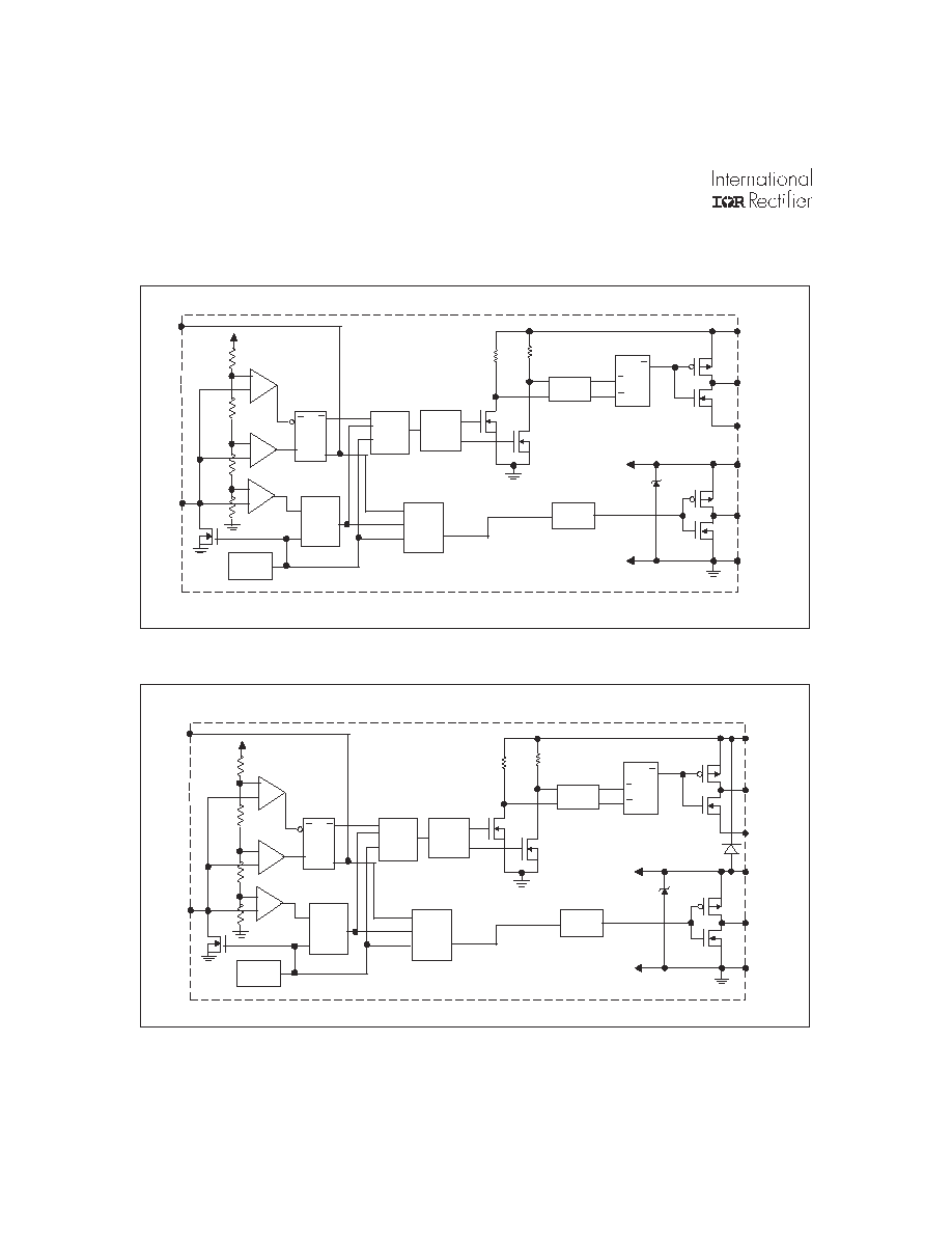
Functional Block Diagram for IR21531(S)
Functional Block Diagram for IR21531D
V
B
PULSE
GEN
DELAY
HV
LEVEL
SHIFT
V
CC
PULSE
FILTER
DEAD
TIME
LO
V
S
COM
R
S
Q
15.6V
C
T
R
T
UV
DETECT
R
Q
S
Q
DEAD
TIME
HO
LOGIC
-
-
-
+
+
+
R
R
R/2
R/2
D1
NOTE: The D1 is a separate die.
V
B
PULSE
GEN
DELAY
HV
LEVEL
SHIFT
V
CC
PULSE
FILTER
DEAD
TIME
LO
V
S
COM
R
S
Q
15.6V
C
T
R
T
UV
DETECT
R
Q
S
Q
DEAD
TIME
HO
LOGIC
-
-
-
+
+
+
R
R
R/2
R/2
IR21531D(S) & (PbF)
www.irf.com
7
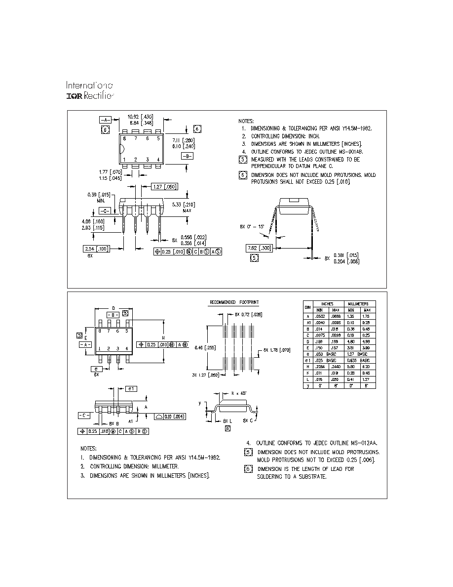
8 Lead SOIC
01-0021 08
8 Lead PDIP
01-3003 01
IR21531D(S) & (PbF)
8
www.irf.com
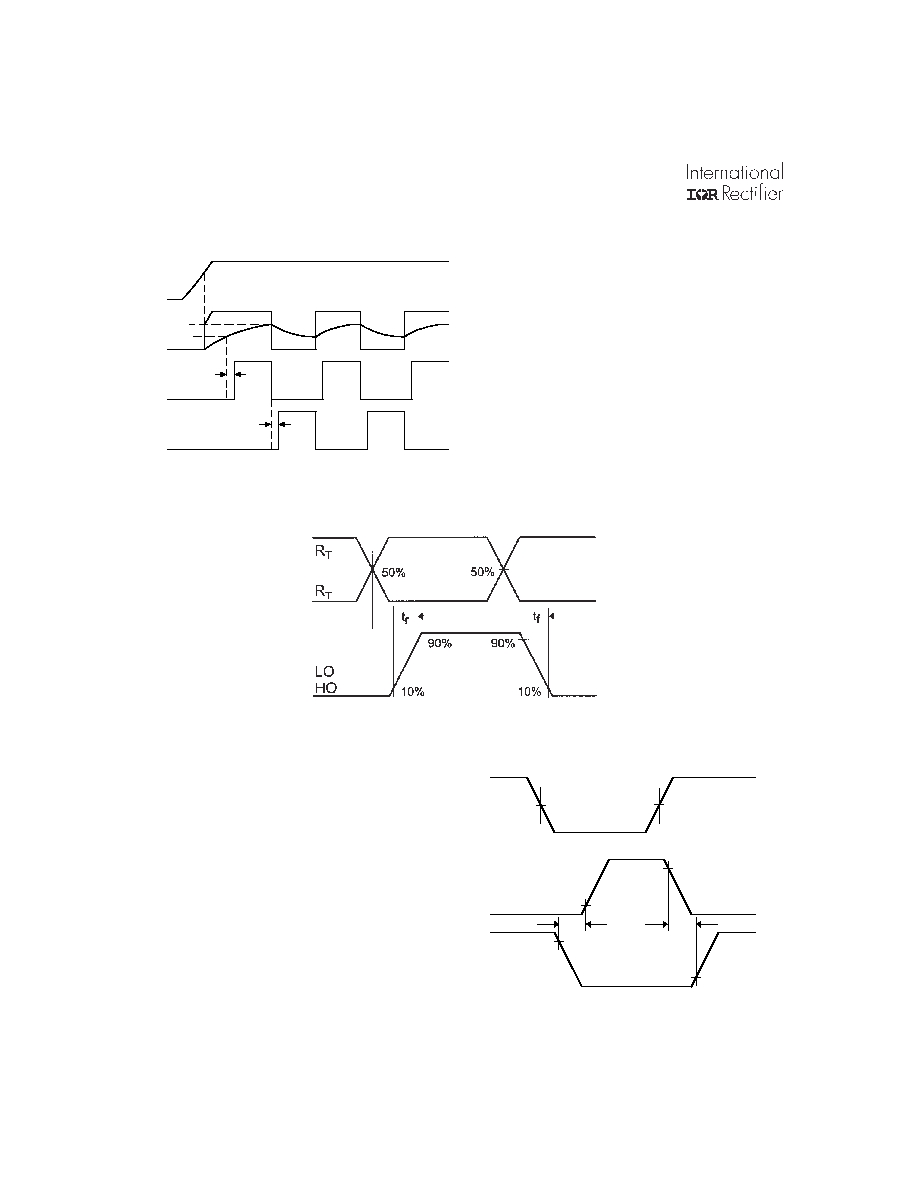
Figure 1. Input/Output Timing Diagram
Figure 3. Deadtime Waveform Definitions
R
T
HO
50%
50%
90%
10%
LO
90%
10%
DT
LO
R
T
C
T
Vcc
Vccuv+
V
CLAMP
R
T
,C
T
1/3
2/3
HO
td
td
Figure 2. Switching Time Waveform Definitions
(HO)
(LO)
IR21531D(S) & (PbF)
www.irf.com
9
LEADFREE PART MARKING INFORMATION
ORDER INFORMATION
Lead Free Released
Non-Lead Free
Released
Part number
Date code
IRxxxxxx
YWW?
?XXXX
Pin 1
Identifier
IR logo
Lot Code
(Prod mode - 4 digit SPN code)
Assembly site code
Per SCOP 200-002
P
?
MARKING CODE
Basic Part (Non-Lead Free)
8-Lead PDIP IR21531D order IR21531D
8-Lead SOIC IR21531S order IR21531S
Leadfree Part
8-Lead PDIP IR21531D order IR21531DPbF
8-Lead SOIC IR21531S order IR21531SPbF
IR WORLD HEADQUARTERS: 233 Kansas St., El Segundo, California 90245 Tel: (310) 252-7105
This product has been qualified per industrial level
Data and specifications subject to change without notice. 4/2/2004