Features
n
Floating channel designed for bootstrap operation
Fully operational to +600V
Tolerant to negative transient voltage
dV/dt immune
n
Undervoltage lockout
n
Programmable oscillator frequency
f
=
Î
+
Î
1
1.4 (R
75 ) C
T
T
n
Matched propagation delay for both channels
n
Low side output in phase with R
T
Description
The IR2151 is a high voltage, high speed, self-os-
cillating power MOSFET and IGBT driver with both high
and low side referenced output channels. Proprietary
HVIC and latch immune CMOS technologies enable
ruggedized monolithic construction. The front end fea-
tures a programmable oscillator which is similar to the
555 timer. The output drivers feature a high pulse cur-
rent buffer stage and an internal deadtime designed for
minimum driver cross-conduction. Propagation delays
for the two channels are matched to simplify use in
50% duty cycle applications. The floating channel can
be used to drive an N-channel power MOSFET or IGBT
in the high side configuration that operates off a high
voltage rail up to 600 volts.
Data Sheet No. PD-6.034G
IR2151
SELF-OSCILLATING HALF-BRIDGE DRIVER
Product Summary
V
OFFSET
600V max.
Duty Cycle
50%
I
O
+/-
100 mA / 210 mA
V
OUT
10 - 20V
Deadtime (typ.)
1.2 Ás
Packages
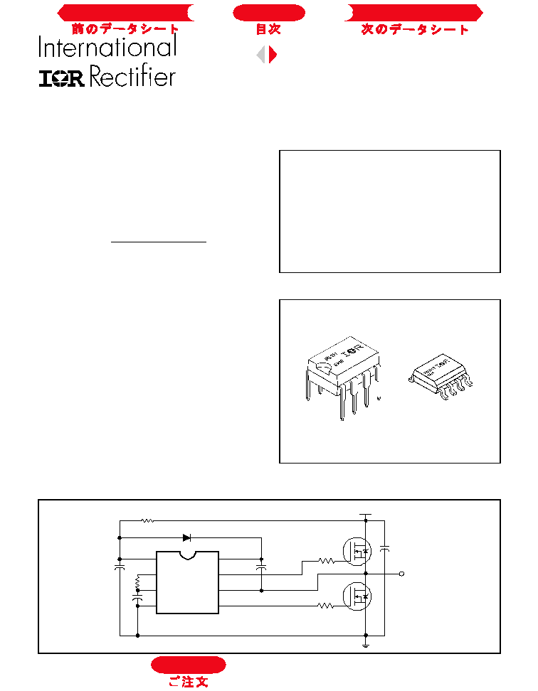
Typical Connection
u p t o 6 0 0 V
V
CC
V
B
V
S
H O
L O
C O M
R
T
C
T
T O
L O A D
C
ONTROL
I
NTEGRATED
C
IRCUIT
D
ESIGNERS
M
ANUAL
B-187
Next Data Sheet
Index
Previous Datasheet
To Order
IR2151
B-188 C
ONTROL
I
NTEGRATED
C
IRCUIT
D
ESIGNERS
M
ANUAL
Parameter
Value
Symbol
Definition
Min.
Max.
Units
V
B
High Side Floating Supply Absolute Voltage
V
S
+ 10
V
S
+ 20
V
S
High Side Floating Supply Offset Voltage
--
600
V
HO
High Side Floating Output Voltage
V
S
V
B
V
LO
Low Side Output Voltage
0
V
CC
I
CC
Supply Current (Note 1)
--
5
mA
T
A
Ambient Temperature
-40
125
░C
Parameter
Value
Symbol
Definition
Min.
Max.
Units
V
B
High Side Floating Supply Voltage
-0.3
625
V
S
High Side Floating Supply Offset Voltage
V
B
- 25
V
B
+ 0.3
V
HO
High Side Floating Output Voltage
V
S
- 0.3
V
B
+ 0.3
V
LO
Low Side Output Voltage
-0.3
V
CC
+ 0.3
V
RT
R
T
Voltage
-0.3
V
CC
+ 0.3
V
CT
C
T
Voltage
-0.3
V
CC
+ 0.3
I
CC
Supply Current (Note 1)
--
25
I
RT
R
T
Output Current
-5
5
dV
s
/dt
Allowable Offset Supply Voltage Transient
--
50
V/ns
P
D
Package Power Dissipation @ T
A
+25░C
(8 Lead DIP)
--
1.0
(8 Lead SOIC)
--
0.625
R
JA
Thermal Resistance, Junction to Ambient
(8 Lead DIP)
--
125
(8 Lead SOIC)
--
200
T
J
Junction Temperature
--
150
T
S
Storage Temperature
-55
150
░C
T
L
Lead Temperature (Soldering, 10 seconds)
--
300
Absolute Maximum Ratings
Absolute Maximum Ratings indicate sustained limits beyond which damage to the device may occur. All voltage param-
eters are absolute voltages referenced to COM. The Thermal Resistance and Power Dissipation ratings are measured
under board mounted and still air conditions.
Recommended Operating Conditions
The Input/Output logic timing diagram is shown in Figure 1. For proper operation the device should be used within the
recommended conditions. The V
S
offset rating is tested with all supplies biased at 15V differential.
V
░C/W
W
mA
V
structure between the chip V
CC
and COM which has a nominal breakdown voltage of 15.6V. Therefore, the IC
supply voltage is normally derived by forcing current into the supply lead (typically by means of a high value
resistor connected between the chip V
CC
and the rectified line voltage and a local decoupling capacitor from
V
CC
to COM) and allowing the internal zener clamp circuit to determine the nominal supply voltage. There-
fore, this circuit should not be driven by a DC, low impedance power source of greater than V
CLAMP
.
Note 1:
Because of the IR2151's application specificity toward off-line supply systems, this IC contains a zener clamp
Next Data Sheet
Index
Previous Datasheet
To Order

IR2151
C
ONTROL
I
NTEGRATED
C
IRCUIT
D
ESIGNERS
M
ANUAL
B-189
Parameter
Value
Symbol
Definition
Min.
Typ. Max. Units Test Conditions
t
r
Turn-On Rise Time
--
80
120
t
f
Turn-Off Fall Time
--
40
70
DT
Deadtime
0.50
1.20
2.25
Ás
D
R
T
Duty Cycle
48
50
52
%
Dynamic Electrical Characteristics
V
BIAS
(V
CC
, V
BS
) = 12V, C
L
= 1000 pF and T
A
= 25░C unless otherwise specified.
ns
Parameter
Value
Symbol
Definition
Min.
Typ. Max. Units Test Conditions
f
OSC
Oscillator Frequency
19.4
20.0
20.6
R
T
= 35.7 k
94
100
106
R
T
= 7.04 k
V
CLAMP
V
CC
Zener Shunt Clamp Voltage
14.4
15.6
16.8
I
CC
= 5 mA
V
CT+
2/3 V
CC
Threshold
7.8
8.0
8.2
V
V
CT-
1/3 V
CC
Threshold
3.8
4.0
4.2
V
CTUV
C
T
Undervoltage Lockout
--
20
50
2.5V<V
CC
<V
CCUV+
V
RT+
R
T
High Level Output Voltage, V
CC
- R
T
--
0
100
I
RT
= -100 ÁA
--
200
300
I
RT
= -1 mA
V
RT-
R
T
Low Level Output Voltage
--
20
50
I
RT
= 100 ÁA
--
200
300
I
RT
= 1 mA
V
RTUV
R
T
Undervoltage Lockout, V
CC
- R
T
--
0
100
2.5V<V
CC
<V
CCUV+
V
OH
High Level Output Voltage, V
BIAS
- V
O
--
--
100
I
O
= 0A
V
OL
Low Level Output Voltage, V
O
--
--
100
I
O
= 0A
I
LK
Offset Supply Leakage Current
--
--
50
V
B
= V
S
= 600V
I
QBS
Quiescent V
BS
Supply Current
--
10
50
I
QCC
Quiescent V
CC
Supply Current
--
400
950
I
CT
C
T
Input Current
--
0.001
1.0
V
CCUV+
V
CC
Supply Undervoltage Positive Going
7.7
8.4
9.2
Threshold
V
CCUV-
V
CC
Supply Undervoltage Negative Going
7.4
8.1
8.9
Threshold
V
CCUVH
V
CC
Supply Undervoltage Lockout Hysteresis
200
500
--
mV
I
O+
Output High Short Circuit Pulsed Current
100
125
--
V
O
= 0V
I
O-
Output Low Short Circuit Pulsed Current
210
250
--
V
O
= 15V
Static Electrical Characteristics
V
BIAS
(V
CC
, V
BS
) = 12V, C
L
= 1000 pF, C
T
= 1 nF and T
A
= 25░C unless otherwise specified. The V
IN
, V
TH
and I
IN
parameters are referenced to COM. The V
O
and I
O
parameters are referenced to COM and are applicable to the
respective output leads: HO or LO.
kHz
mV
V
mA
ÁA
Next Data Sheet
Index
Previous Datasheet
To Order
IR2151
B-190 C
ONTROL
I
NTEGRATED
C
IRCUIT
D
ESIGNERS
M
ANUAL
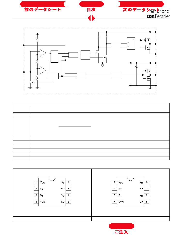
Lead Definitions
Lead
Symbol
Description
R
T
Oscillator timing resistor input,in phase with LO for normal IC operation
C
T
Oscillator timing capacitor input, the oscillator frequency according to the following equation:
f
=
Î
+
Î
1
1.4 (R
75 ) C
T
T
where 75
is the effective impedance of the R
T
output stage
V
B
High side floating supply
HO
High side gate drive output
V
S
High side floating supply return
V
CC
Low side and logic fixed supply
LO
Low side gate drive output
COM
Low side return
Functional Block Diagram
Lead Assignments
8 Lead DIP
SO-8
IR2151
IR2151S
V
B
PULSE
GEN
DELAY
HV
LEVEL
SHIFT
V
CC
PULSE
FILTER
DEAD
TIME
LO
HO
V
S
COM
R
S
Q
15.6V
C
T
R
T
UV
DETECT
+
-
+
-
R
Q
S
Q
R
R
R
DEAD
TIME
Next Data Sheet
Index
Previous Datasheet
To Order
IR2151
C
ONTROL
I
NTEGRATED
C
IRCUIT
D
ESIGNERS
M
ANUAL
B-191
Thickness of Gate Oxide
800
┼
Connections
Material
Poly Silicon
First
Width
5 Ám
Layer
Spacing
6 Ám
Thickness
5000┼
Material
Al - Si - Cu (Si: 1.0%, Cu ▒0.5%)
Second
Width
6 Ám
Layer
Spacing
9 Ám
Thickness
20,000┼
Contact Hole Dimension
5 Ám X 5 Ám
Insulation Layer
Material
PSG (SiO
2
)
Thickness
1.7 Ám
Passivation
Material
PSG (SiO
2
)
Thickness
1.7 Ám
Method of Saw
Full Cut
Method of Die Bond
Ablebond 84 - 1
Wire Bond
Method
Thermo Sonic
Material
Au (1.0 mil / 1.3 mil)
Leadframe
Material
Cu
Die Area
Ag
Lead Plating
Pb : Sn (37 : 63)
Package
Types
8 Lead PDIP / SO-8
Materials
EME6300 / MP150 / MP190
Remarks:
Device Information
Process & Design Rule
HVDCMOS 4.0 Ám
Transistor Count
231
Die Size
68 X 101 X 26 (mil)
Die Outline
Next Data Sheet
Index
Previous Datasheet
To Order