Data Sheet No. PD60046-S
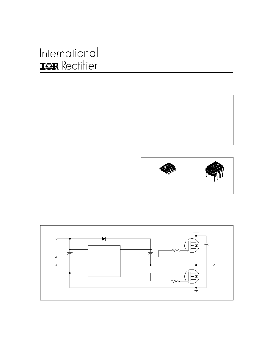
Typical Connection
Product Summary
V
OFFSET
600V max.
I
O
+/-
130 mA / 270 mA
V
OUT
10 - 20V
t
on/off
(typ.)
680 & 150 ns
Deadtime (typ.)
520 ns
HALF-BRIDGE DRIVER
Features
·
Floating channel designed for bootstrap operation
Fully operational to +600V
Tolerant to negative transient voltage
dV/dt immune
·
Gate drive supply range from 10 to 20V
·
Undervoltage lockout
·
3.3V, 5V and 15V input logic compatible
·
Cross-conduction prevention logic
·
Internally set deadtime
·
High side output in phase with input
·
Shut down input turns off both channels
·
Matched propagation delay for both channels
·
Also available LEAD-FREE
Description
The IR2104(S) are high voltage, high speed power
MOSFET and IGBT drivers with dependent high and low
side referenced output channels. Proprietary HVIC and
latch immune CMOS technologies enable ruggedized
monolithic construction. The logic input is compatible with standard CMOS or LSTTL output, down to 3.3V logic.
The output drivers feature a high pulse current buffer stage designed for minimum driver cross-conduction. The
floating channel can be used to drive an N-channel power MOSFET or IGBT in the high side configuration which
operates from 10 to 600 volts.
www.irf.com
1
IR2104
(S) & (PbF)
V
CC
V
B
V
S
HO
LO
COM
IN
SD
SD
IN
up to 600V
TO
LOAD
V
CC
(Refer to Lead Assignment for correct pin configuration) This/These diagram(s) show electrical
connections only. Please refer to our Application Notes and DesignTips for proper circuit board layout.
Packages
8 Lead PDIP
IR2104
8 Lead SOIC
IR2104S
2
IR2104
(S) & (PbF)
www.irf.com
Symbol
Definition
Min.
Max.
Units
V
B
High side floating absolute voltage
-0.3
625
V
S
High side floating supply offset voltage
V
B
- 25
V
B
+ 0.3
V
HO
High side floating output voltage
V
S
- 0.3
V
B
+ 0.3
V
CC
Low side and logic fixed supply voltage
-0.3
25
V
LO
Low side output voltage
-0.3
V
CC
+ 0.3
V
IN
Logic input voltage (IN &
SD
)
-0.3
V
CC
+ 0.3
dV
s
/dt
Allowable offset supply voltage transient
--
50
V/ns
P
D
Package power dissipation @ T
A
+25
°C
(8 lead PDIP)
--
1.0
(8 lead SOIC)
--
0.625
Rth
JA
Thermal resistance, junction to ambient
(8 lead PDIP)
--
125
(8 lead SOIC)
--
200
T
J
Junction temperature
--
150
T
S
Storage temperature
-55
150
T
L
Lead temperature (soldering, 10 seconds)
--
300
Absolute Maximum Ratings
Absolute maximum ratings indicate sustained limits beyond which damage to the device may occur. All voltage
parameters are absolute voltages referenced to COM. The thermal resistance and power dissipation ratings are
measured under board mounted and still air conditions.
Symbol
Definition
Min.
Max.
Units
V
B
High side floating supply absolute voltage
V
S
+ 10
V
S
+ 20
V
S
High side floating supply offset voltage
Note 1
600
V
HO
High side floating output voltage
V
S
V
B
V
CC
Low side and logic fixed supply voltage
10
20
V
LO
Low side output voltage
0
V
CC
V
IN
Logic input voltage (IN &
SD
)
0
V
CC
T
A
Ambient temperature
-40
125
Note 1: Logic operational for V
S
of -5 to +600V. Logic state held for V
S
of -5V to -V
BS
. (Please refer to the Design Tip
DT97-3 for more details).
Recommended Operating Conditions
The Input/Output logic timing diagram is shown in Figure 1. For proper operation the device should be used within the
recommended conditions. The V
S
offset rating is tested with all supplies biased at 15V differential.
°C
V
V
W
°C/W
°C
3
IR2104
(S) & (PbF)
www.irf.com
Symbol
Definition
Min. Typ. Max. Units Test Conditions
V
IH
Logic "1" (HO) & Logic "0" (LO) input voltage
3
--
--
V
CC
= 10V to 20V
V
IL
Logic "0" (HO) & Logic "1" (LO) input voltage
--
--
0.8
V
CC
= 10V to 20V
V
SD,TH+
SD input positive going threshold
3
--
--
V
CC
= 10V to 20V
V
SD,TH-
SD input negative going threshold
--
--
0.8
V
CC
= 10V to 20V
V
OH
High level output voltage, V
BIAS
- V
O
--
--
100
I
O
= 0A
V
OL
Low level output voltage, V
O
--
--
100
I
O
= 0A
I
LK
Offset supply leakage current
--
--
50
V
B
= V
S
= 600V
I
QBS
Quiescent V
BS
supply current
--
30
55
V
IN
= 0V or 5V
I
QCC
Quiescent V
CC
supply current
--
150
270
V
IN
= 0V or 5V
I
IN+
Logic "1" input bias current
--
3
10
V
IN
= 5V
I
IN-
Logic "0" input bias current
--
--
1
V
IN
= 0V
V
CCUV+
V
CC
supply undervoltage positive going
8
8.9
9.8
threshold
V
CCUV-
V
CC
supply undervoltage negative going
7.4
8.2
9
threshold
I
O+
Output high short circuit pulsed current
130
210
--
V
O
= 0V
PW
10
µs
I
O-
Output low short circuit pulsed current
270
360
--
V
O
= 15V
PW
10
µs
Symbol
Definition
Min. Typ. Max. Units Test Conditions
ton
Turn-on propagation delay
--
680
820
V
S
= 0V
toff
Turn-off propagation delay
--
150
220
V
S
= 600V
tsd
Shutdown propagation delay
--
160
220
tr
Turn-on rise time
--
100
170
tf
Turn-off fall time
--
50
90
DT
Deadtime, LS turn-off to HS turn-on &
400
520
650
HS turn-on to LS turn-off
Static Electrical Characteristics
V
BIAS
(V
CC
, V
BS
) = 15V and T
A
= 25
°C unless otherwise specified. The V
IN
, V
TH
and I
IN
parameters are referenced to
COM. The V
O
and I
O
parameters are referenced to COM and are applicable to the respective output leads: HO or LO.
Dynamic Electrical Characteristics
V
BIAS
(V
CC
, V
BS
) = 15V, C
L
= 1000 pF and T
A
= 25
°C unless otherwise specified.
V
mV
V
mA
MT
Delay matching, HS & LS turn-on/off
--
--
60
ns
µA
4
IR2104
(S) & (PbF)
www.irf.com
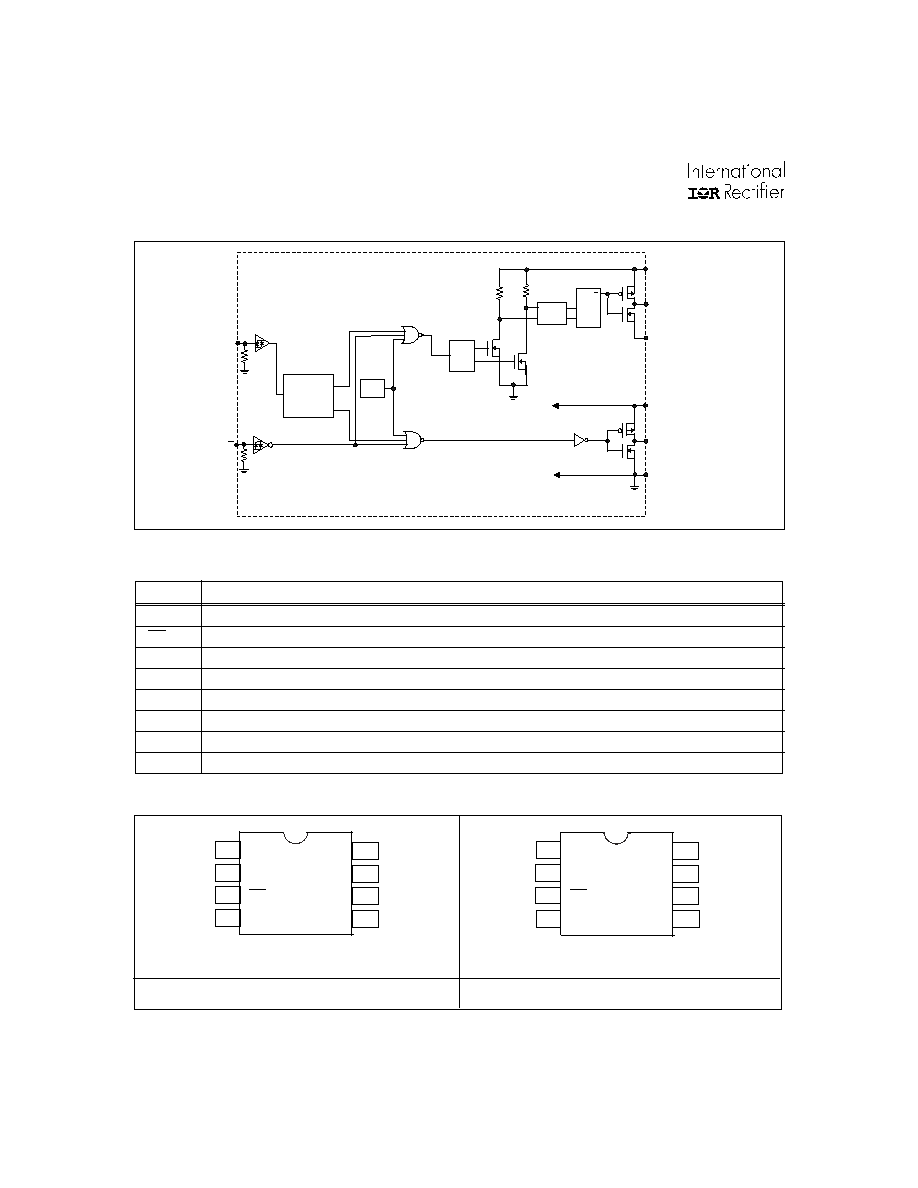
Functional Block Diagram
Lead Definitions
Symbol Description
IN
Logic input for high and low side gate driver outputs (HO and LO), in phase with HO
Logic input for shutdown
V
B
High side floating supply
HO
High side gate drive output
V
S
High side floating supply return
V
CC
Low side and logic fixed supply
LO
Low side gate drive output
COM
Low side return
SD
Lead Assignments
8 Lead PDIP
8 Lead SOIC
IR2104
IR2104S
1
2
3
4
8
7
6
5
VCC
IN
SD
COM
VB
HO
VS
LO
1
2
3
4
8
7
6
5
VCC
IN
SD
COM
VB
HO
VS
LO
VB
HO
VS
IN
SD
DEAD TIME &
SHOOT-THROUGH
PREVENTION
PULSE
GEN
PULSE
FILTER
HV
LEVEL
SHIFT
R
S
Q
VCC
LO
COM
UV
DETECT

5
IR2104
(S) & (PbF)
www.irf.com
Figure 5. Delay Matching Waveform Definitions
HO
50%
50%
10%
LO
90%
MT
HO
LO
MT
IN
(LO)
IN
(HO)
Figure 4. Deadtime Waveform Definitions
IN
HO
50%
50%
90%
10%
LO
90%
10%
DT
DT
Figure 3. Shutdown Waveform Definitions
SD
tsd
HO
LO
50%
90%
Figure 1. Input/Output Timing Diagram
SD
IN
HO
LO
Figure 2. Switching Time Waveform Definitions
IN
(HO)
tr
ton
tf
toff
LO
HO
50%
50%
90%
90%
10%
10%
IN
(LO)
6
IR2104
(S) & (PbF)
www.irf.com
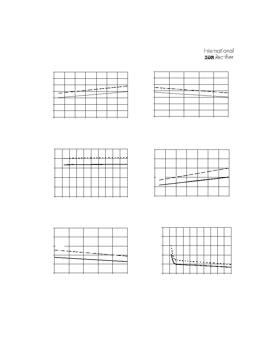
Figure 6A. Turn-On Time vs Temperature
Figure 6B. Turn-On Time vs Supply Voltage
Figure 7A. Turn-Off Time vs Temperature
Figure 7B. Turn-Off Time vs Supply Voltage
Temperature (°C)
VBIAS Supply Voltage (V)
Temperature (°C)
VBIAS Supply Voltage (V)
Turn-Off Delay Time (ns)
0
100
200
300
400
500
10
12
14
16
18
20
Max.
Typ.
Turn-Off Delay Time (ns)
0
2 0 0
4 0 0
6 0 0
8 0 0
1 0 0 0
1 2 0 0
1 4 0 0
-5 0
-2 5
0
2 5
5 0
7 5
1 0 0
1 2 5
T
u
rn
-O
n
D
e
l
ay
T
i
me
(
n
s
)
M a x.
T yp .
Turn-On Delay Time (ns)
0
200
400
600
800
1000
1200
1400
10
12
14
16
18
20
Max.
Typ.
0
1 0 0
2 0 0
3 0 0
4 0 0
5 0 0
-5 0
-2 5
0
2 5
5 0
7 5
1 0 0
1 2 5
M a x .
T y p .
0
200
400
600
800
1000
0
2
4
6
8
10
12
14
16
18
20
Turn-On Delay Time (ns
)
Max.
Typ
.
0
200
400
600
800
1000
0
2
4
6
8
10 12 14 16 18 20
Turn-Off Delay Time (ns
Max.
Typ
Figure 7C. Turn-Off Time vs Input Voltage
Figure 6C. Turn-On Time vs Input Voltage
Input Voltage (V)
Input Voltage (V)

7
IR2104
(S) & (PbF)
www.irf.com
Figure 8A. Shutdown Time vs Temperature
Figure 8B. Shutdown Time vs Voltage
VBIAS Supply Voltage (V)
Temperature (°C)
Shutdown Delay Time (ns)
0
100
200
300
400
500
10
12
14
16
18
20
Max.
Typ.
Shutdown Delay Time (ns)
0
1 0 0
2 0 0
3 0 0
4 0 0
5 0 0
-5 0
-2 5
0
2 5
5 0
7 5
1 0 0
1 2 5
T y p .
M a x .
Figure 10A. Turn-Off Fall Time
vs Temperature
Temperature (°C)
VBIAS Supply Voltage (V)
Figure 10B. Turn-Off Fall Time vs Voltage
Turn-Off Fall Time (ns)
0
5 0
1 0 0
1 5 0
2 0 0
1 0
1 2
1 4
1 6
1 8
2 0
M a x .
T y p .
Turn-Off Fall Time (ns)
Figure 9A. Turn-On Rise Time
vs Temperature
Figure 9B. Turn-On Rise Time vs Voltage
Temperature (°C)
VBIAS Supply Voltage (V)
0
1 0 0
2 0 0
3 0 0
4 0 0
5 0 0
-5 0
-2 5
0
2 5
5 0
7 5
1 0 0
1 2 5
M a x .
T y p .
Turn-On Rise Time (ns)
0
1 0 0
2 0 0
3 0 0
4 0 0
5 0 0
1 0
1 2
1 4
1 6
1 8
2 0
M a x .
T y p .
Turn-On Rise Time (ns)
0
5 0
1 0 0
1 5 0
2 0 0
-5 0
-2 5
0
2 5
5 0
7 5
1 0 0
1 2 5
M a x .
T y p .

8
IR2104
(S) & (PbF)
www.irf.com
Temperature (°C)
Figure 12A. Logic "1" (HO) & Logic "0" (LO)
& Inactive SD Input Voltage
vs Temperature
Figure 12B. Logic "1" (HO) & Logic "0" (LO)
& Inactive SD Input Voltage
vs Voltage
Figure 13A. Logic "0" (HO) & Logic "1" (LO)
& Active SD Input Voltage
vs Temperature
Temperature (°C)
Vcc Supply Voltage (V)
Figure 13B. Logic "0" (HO) & Logic "1" (LO)
& Active SD Input Voltage
vs Voltage
Vcc Supply Voltage (V)
0
1
2
3
4
5
6
7
8
-5 0
-2 5
0
2 5
5 0
7 5
1 0 0
1 2 5
I
nput
V
o
l
ta
g
e
(
V
)
M in .
0
0 .8
1 .6
2 .4
3 .2
4
1 0
1 2
1 4
1 6
1 8
2 0
I
nput
V
o
l
t
age
(
V
)
M a x .
0
1
2
3
4
5
6
7
8
1 0
1 2
1 4
1 6
1 8
2 0
I
np
ut
V
o
l
t
age
(
V
)
M in .
0
0.8
1.6
2.4
3.2
4
-50
-25
0
25
50
75
100
125
I
n
p
u
t
V
o
l
t
a
ge
(
V
)
Max.
Temperature (°C)
VBIAS Supply Voltage (V)
Deadtime (ns)
Figure 11A. Deadtime vs Temperature
Deadtime (ns)
Figure 11B. Deadtime vs Voltage
0
2 0 0
4 0 0
6 0 0
8 0 0
1 0 0 0
1 2 0 0
1 4 0 0
-5 0
-2 5
0
2 5
5 0
7 5
1 0 0
1 2 5
M a x .
T y p .
M in .
0
2 0 0
4 0 0
6 0 0
8 0 0
1 0 0 0
1 2 0 0
1 4 0 0
1 0
1 2
1 4
1 6
1 8
2 0
M a x .
T y p .
M in .
9
IR2104
(S) & (PbF)
www.irf.com
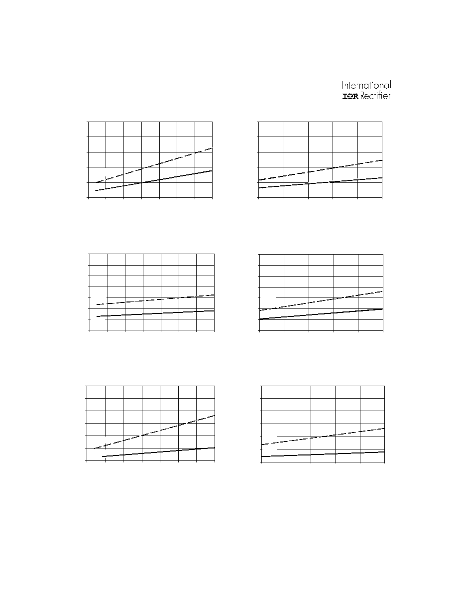
Temperature (°C)
Vcc Supply Voltage (V)
Figure 14A. High Level Output
vs Temperature
Figure 14B. High Level Output vs Voltage
0
0 .2
0 .4
0 .6
0 .8
1
1 0
1 2
1 4
1 6
1 8
2 0
M a x .
High Level Output V
oltage (V)
0
0 .2
0 .4
0 .6
0 .8
1
-5 0
-2 5
0
2 5
5 0
7 5
1 0 0
1 2 5
M a x .
High Level Output V
oltage (V)
Figure 15A. Low Level Output
vs Temperature
Temperature (°C)
Vcc Supply Voltage (V)
Figure 15B. Low level Output vs Voltage
Offset Supply Leakage Current (
µ
A)
Temperature (°C)
Figure 16A. Offset Supply Current
vs Temperature
Low Level Output V
oltage (V)
0
0 .2
0 .4
0 .6
0 .8
1
1 0
1 2
1 4
1 6
1 8
2 0
M a x .
Offset Supply Leakage Current (
µ
A)
Figure 16B. Offset Supply Current
vs Voltage
0
0 .2
0 .4
0 .6
0 .8
1
-5 0
-2 5
0
2 5
5 0
7 5
1 0 0
1 2 5
M a x .
Low Level Output V
oltage (V)
0
1 0 0
2 0 0
3 0 0
4 0 0
5 0 0
-5 0
-2 5
0
2 5
5 0
7 5
1 0 0
1 2 5
M a x .
0
100
200
300
400
500
0
100
200
300
400
500
600
Max.
VB Boost Voltage (V)
10
IR2104
(S) & (PbF)
www.irf.com
Figure 18A. Vcc Supply Current
vs Temperature
Vcc Supply Current (
µ
A)
Vcc Supply Current (
µ
A)
Figure 18B. Vcc Supply Current vs Voltage
Vcc Supply Voltage (V)
Figure 19A. Logic"1" Input Current
vs Temperature
Temperature (°C)
Logic 1" Input Current (
µ
A)
Logic 1" Input Current (
µ
A)
Figure 19B. Logic"1" Input Current
vs Voltage
0
1 0 0
2 0 0
3 0 0
4 0 0
5 0 0
6 0 0
7 0 0
1 0
1 2
1 4
1 6
1 8
2 0
M a x .
T y p .
0
5
1 0
1 5
2 0
2 5
3 0
-5 0
-2 5
0
2 5
5 0
7 5
1 0 0
1 2 5
M a x .
T y p .
0
5
1 0
1 5
2 0
2 5
3 0
1 0
1 2
1 4
1 6
1 8
2 0
M a x .
T y p .
Vcc Supply Voltage (V)
0
1 0 0
2 0 0
3 0 0
4 0 0
5 0 0
6 0 0
7 0 0
-5 0
-2 5
0
2 5
5 0
7 5
1 0 0
1 2 5
M a x .
T y p .
Temperature (°C)
Figure 17A. V
BS
Supply Current
vs Temperature
Figure 17B. V
BS
Supply Current
vs Voltage
VBS Floating Supply Voltage (V)
Temperature (°C)
VBS Supply Current (
µ
A)
VBS Supply Current (
µ
A)
0
30
60
90
120
150
10
12
14
16
18
20
Max.
Ty p.
0
3 0
6 0
9 0
1 2 0
1 5 0
-5 0
-2 5
0
2 5
5 0
7 5
1 0 0
1 2 5
M a x .
T y p .
11
IR2104
(S) & (PbF)
www.irf.com
Logic "0" Input Current (
µ
A)
Figure 20A. Logic "0" Input Current
vs Temperature
Temperature (°C)
VCC Supply Voltage (V)
Figure 20B. Logic "0" Input Current
vs Voltage
0
1
2
3
4
5
10
12
14
16
18
20
Log
i
c
"
0
"
I
npu
t
C
u
r
r
ent
(
u
A
)
Max.
0
1
2
3
4
5
-50
-25
0
25
50
75
100
125
Max.
VCC UVLO Threshold +(V)
Figure 21A. Vcc Undervoltage Threshold(+)
vs Temperature
Temperature (°C)
Figure 21B. Vcc Undervoltage Threshold(-)
vs Temperature
VCC UVLO Threshold - (V)
Output Source Current (mA)
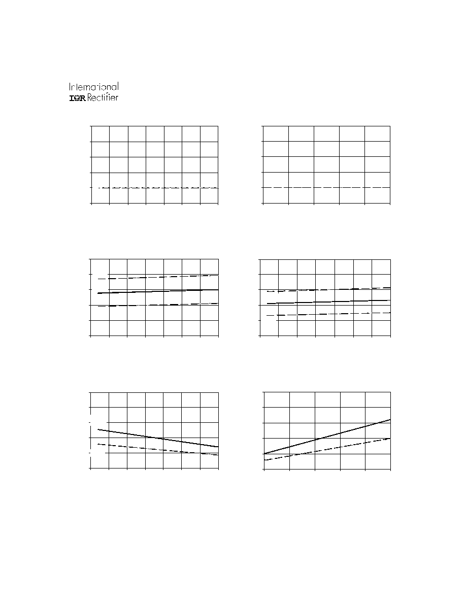
Figure 22A. Output Source Current
vs Temperature
Temperature (°C)
Figure 22B. Output Source Current
vs Voltage
Output Source Current (mA)
6
7
8
9
10
11
-50
-25
0
25
50
75
100
125
Max.
Min.
Typ.
0
100
200
300
400
500
-50
-25
0
25
50
75
100
125
Typ.
Min.
6
7
8
9
1 0
1 1
-5 0
-2 5
0
2 5
5 0
7 5
1 0 0
1 2 5
M a x .
M in .
T y p .
Temperature (°C)
0
1 0 0
2 0 0
3 0 0
4 0 0
5 0 0
1 0
1 2
1 4
1 6
1 8
2 0
T y p .
M in .
VBIAS Supply Voltage (V)
12
IR2104
(S) & (PbF)
www.irf.com
Output Sink Current (mA)
Temperature (°C)
Figure 23A. Output Sink Current
vs Temperature
Figure 23B. Output Sink Current vs Voltage
Output Sink Current (mA)
0
1 0 0
2 0 0
3 0 0
4 0 0
5 0 0
6 0 0
7 0 0
-5 0
-2 5
0
2 5
5 0
7 5
1 0 0
1 2 5
T y p .
M in .
0
1 0 0
2 0 0
3 0 0
4 0 0
5 0 0
6 0 0
7 0 0
1 0
1 2
1 4
1 6
1 8
2 0
T y p .
M in .
VBIAS Supply Voltage (V)
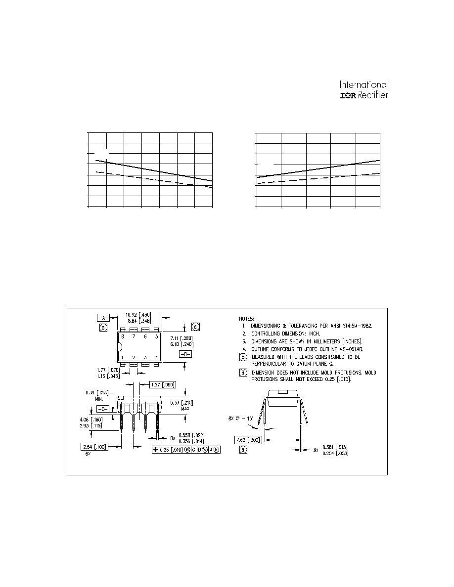
Case Outlines
01-6014
01-3003 01
(MS-001AB)
8 Lead PDIP
13
IR2104
(S) & (PbF)
www.irf.com
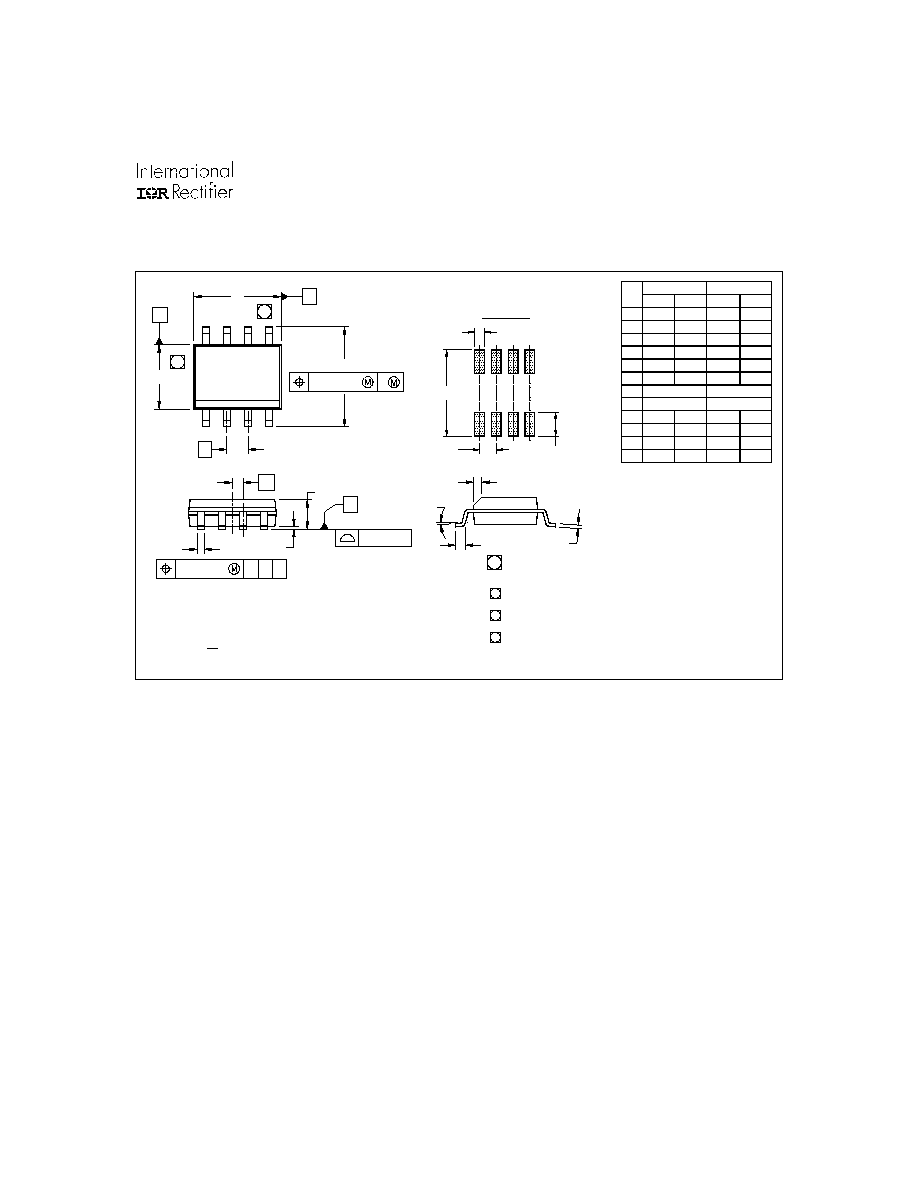
01-6027
01-0021 11
(MS-012AA)
8 Lead SOIC
8
7
5
6
5
D
B
E
A
e
6X
H
0.25 [.010]
A
6
4
3
1
2
4. OUTLINE CONFORMS TO JEDEC OUTLINE MS-012AA.
NOTES:
1. DIMENSIONING & TOLERANCING PER ASME Y14.5M-1994.
2. CONTROLLING DIMENSION: MILLIMETER
3. DIMENSIONS ARE SHOWN IN MILLIMETERS [INCHES].
7
K x 45°
8X L
8X c
y
FOOTPRINT
8X 0.72 [.028]
6.46 [.255]
3X 1.27 [.050]
8X 1.78 [.070]
5 DIMENSION DOES NOT INCLUDE MOLD PROTRUSIONS.
6 DIMENSION DOES NOT INCLUDE MOLD PROTRUSIONS.
MOLD PROTRUSIONS NOT TO EXCEED 0.25 [.010].
7 DIMENSION IS THE LENGTH OF LEAD FOR SOLDERING TO
A SUBSTRATE.
MOLD PROTRUSIONS NOT TO EXCEED 0.15 [.006].
0.25 [.010]
C A B
e1
A
A1
8X b
C
0.10 [.004]
e 1
D
E
y
b
A
A1
H
K
L
.189
.1497
0°
.013
.050 BASIC
.0532
.0040
.2284
.0099
.016
.1968
.1574
8°
.020
.0688
.0098
.2440
.0196
.050
4.80
3.80
0.33
1.35
0.10
5.80
0.25
0.40
0°
1.27 BASIC
5.00
4.00
0.51
1.75
0.25
6.20
0.50
1.27
MIN
MAX
MILLIMETERS
INCHES
MIN
MAX
DIM
8°
e
c
.0075
.0098
0.19
0.25
.025 BASIC
0.635 BASIC
14
IR2104
(S) & (PbF)
www.irf.com
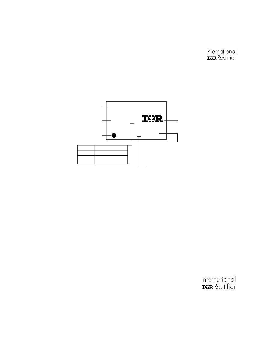
LEADFREE PART MARKING INFORMATION
ORDER INFORMATION
Lead Free Released
Non-Lead Free
Released
Part number
Date code
IRxxxxxx
YWW?
?XXXX
Pin 1
Identifier
IR logo
Lot Code
(Prod mode - 4 digit SPN code)
Assembly site code
Per SCOP 200-002
P
?
MARKING CODE
Basic Part (Non-Lead Free)
8-Lead PDIP IR2104 order IR2104
8-Lead SOIC IR2104S order IR2104S
Leadfree Part
8-Lead PDIP IR2104 order IR2104PbF
8-Lead SOIC IR2104S order IR2104SPbF
IR WORLD HEADQUARTERS: 233 Kansas St., El Segundo, California 90245 Tel: (310) 252-7105
This product has been qualified per industrial level
Data and specifications subject to change without notice. 4/2/2004