Äîêóìåíòàöèÿ è îïèñàíèÿ www.docs.chipfind.ru
Flipky
TM
1 Amp
IR130CSP
Bulletin I0182J 08/05
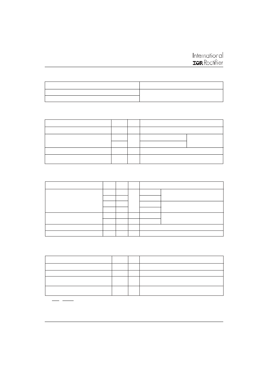
Major Ratings and Characteristics
I
F(AV)
Rectangular waveform
1.0
A
V
RRM
30
V
I
FSM
@ tp = 5 µs sine
220
A
V
F
@
1.0 Apk, T
J
=125°C
0.33
V
T
J
range
- 55 to 150
°C
Characteristics
IR130CPS
Units
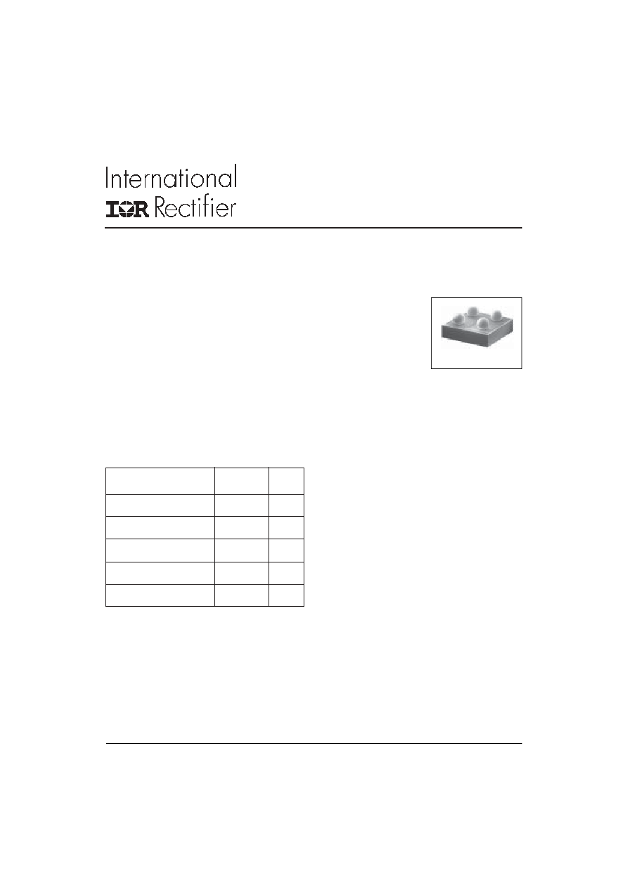
True chip-scale packaging is available from International
Rectifier. The IR130CPS surface-mount Schottky recti-
fier has been designed for applications requiring low
forward drop and very small foot prints on PC boards.
Typical applications are in disk drives, switching power
supplies, converters, free-wheeling diodes, battery
charging, and reverse battery protection.
Small foot print, surface mountable
Low forward voltage drop
High frequency operation
Guard ring for enhanced ruggedness and long term
reliability
The Flipky
TM
package, is one-fifth the footprint of a
comparable SMA package and has a profile of less then
.8mm. Combined with the low thermal resistance of the
die level device, this makes the Flipky
TM
the best device
for application where printed circuit board space is at a
premium and in extremely thin application environments
such as battery packs, cell phones and PCMCIA cards.
Description
Flipky
TM
Ultra Low V
F
per Footprint Area
Low Thermal Resistance
One-fifth Footprint of SMA
Super Low Profile (<.8mm)
Available Tested on Tape & Reel
Features
1
www.irf.com
IR130CSP
Bulletin I0182J 08/05
2
www.irf.com
V
R
Max. DC Reverse Voltage (V)
V
RWM
Max. Working Peak Reverse Voltage (V)
30
Voltage Ratings
(1) Pulse Width < 300µs, Duty Cycle < 2%
I
F(AV)
Max. Average Forward Current
1.0
A
50% duty cycle @ T
PCB
= 120 °C, rectangular wave form
I
FSM
Max. Peak One Cycle Non-Repetitive
220
A
5µs Sine or 3µs Rect. pulse
Surge Current @ 25°C
21
10ms Sine or 6ms Rect. pulse
E
AS
Non- Repetitive Avalanche Energy
10
mJ
T
J
= 25 °C, I
AS
= 2.0A, L = 5.0mH
I
AR
Repetitive Avalanche Current
2.0
A
Current decaying linearly to zero in 1 µsec
Frequency limited by T
J
max. Va = 1.5 x Vr typical
Parameters
Value Units
Conditions
Absolute Maximum Ratings
Following any rated
load condition and
with rated V
RRM
applied
Part number
IR130CSP
T
J
Max. Junction Temperature Range (*)
- 55 to 150
°C
T
stg
Max. Storage Temperature Range
- 55 to 150
°C
R
thJL
Typ. Thermal Resistance Junction
40
°C/W DC operation
to PCB
(**)
R
thJA
Max. Thermal Resistance Junction
62
°C/W
to Ambient
Thermal-Mechanical Specifications
Parameters
Value
Units
Conditions
<
thermal runaway condition for a diode on its own heatsink
(**) Mounted 1 inch square PCB
(*) dPtot
1
dTj
Rth( j-a)
V
FM
Max. Forward Voltage (1)
0.41
0.45
V
@ 1A
T
J
= 25 °C
Drop
0.46
0.50
@ 2A
0.29
0.33
@ 1A
T
J
= 125 °C
0.37
0.40
@ 2A
I
RM
Max. Reverse Leakage (1)
30
100
µA
T
J
= 25 °C
V
R
= rated V
R
Current
10
30
mA
T
J
= 125 °C
C
T
Max. Junction Capacitance
-
210
pF
V
R
= 5V
DC
(test signal range 100kHz to 1MHz) 25°C
dv/dt Max. Volatge Rate of Charge
-
10000 V/ µs (Rated V
R
)
Electrical Specifications
Parameters
Typ.
Max. Units
Conditions
IR130CSP
Bulletin I0182J 08/05
3
www.irf.com
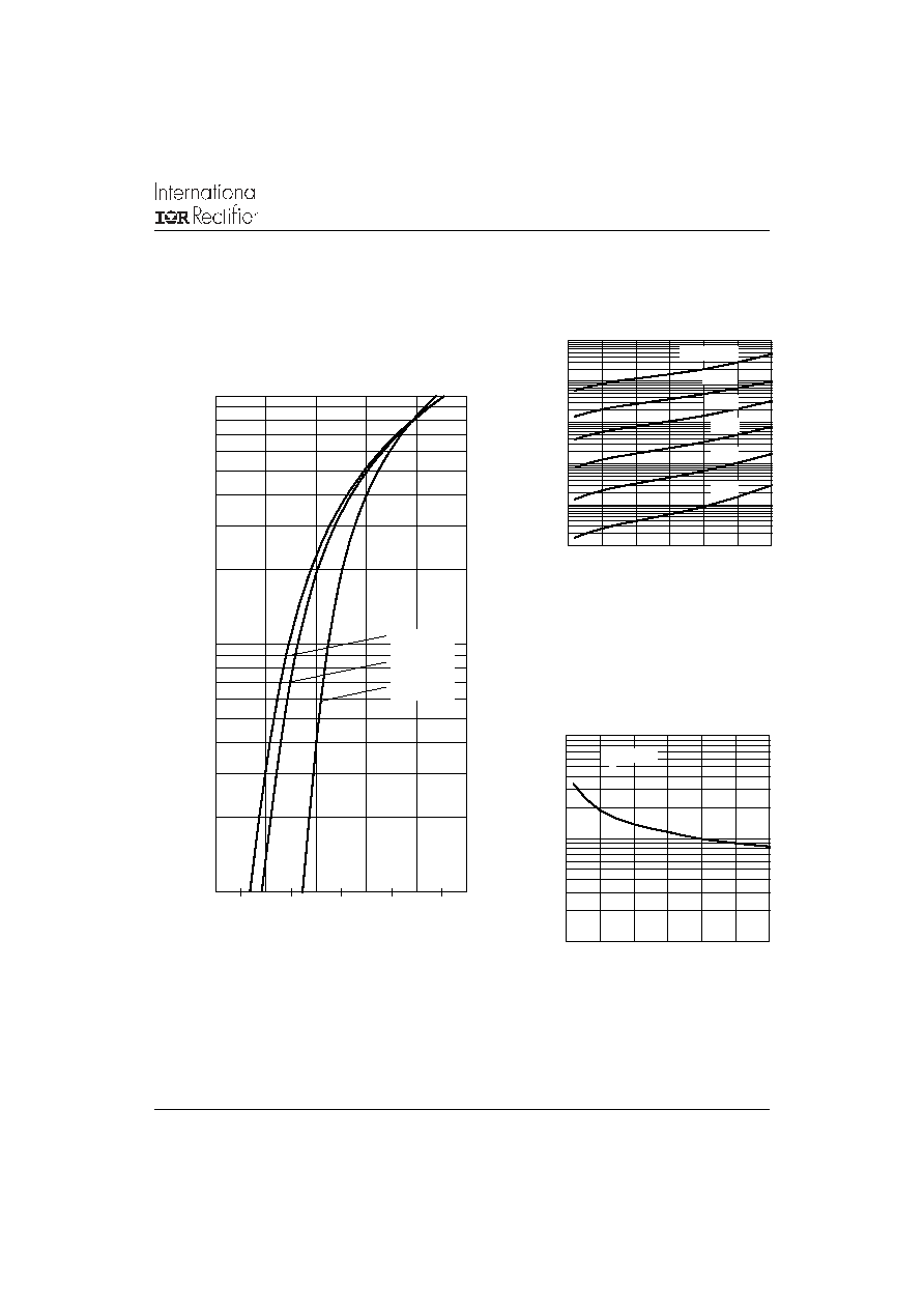
Fig. 2 - Typical Values Of Reverse Current
Vs. Reverse Voltage (Per Leg)
Fig. 3 - Typical Junction Capacitance
Vs. Reverse Voltage (Per Leg)
Fig. 1 - Max. Forward Voltage Drop Characteristics
(Per Leg)
Forward Voltage Drop - V
FM
(V)
Instantaneous Forward Current - I
F
(A)
Reverse Voltage - V
R
(V)
Reverse Current - I
R
(mA)
Reverse Voltage - V
R
(V)
Junction Capacitance - C
T
(p F)
0.1
1
10
0
0.2
0.4
0.6
0.8
1
T = 150°C
T = 125°C
T = 25°C
J
J
J
0.001
0.01
0.1
1
10
100
0
5
10
15
20
25
30
125°C
100°C
75°C
50°C
25°C
Tj = 150°C
10
100
1000
0
5
10
15
20
25
30
T = 25°C
J
IR130CSP
Bulletin I0182J 08/05
4
www.irf.com
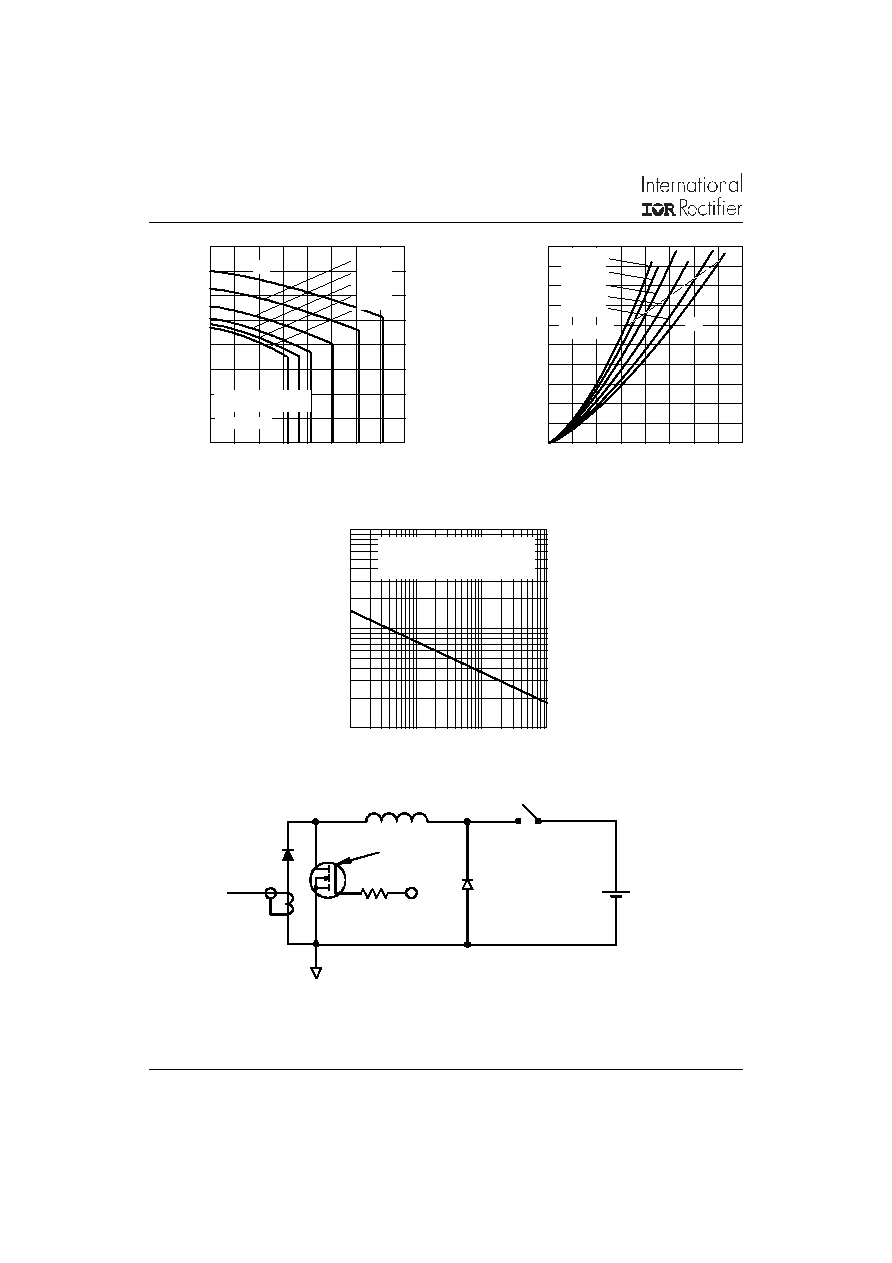
Fig. 6 - Max. Non-Repetitive Surge Current (Per Leg)
Fig. 4 - Max. Allowable Case Temperature
Vs. Average Forward Current (Per Leg)
Fig. 8 - Unclamped Inductive Test Circuit
Fig. 5 - Forward Power Loss Characteristics
(Per Leg)
FREE-WHEEL
DIODE
40HFL40S02
CURRENT
MONITOR
HIGH-SPEED
SWITCH
IRFP460
L
DUT
Rg = 25 ohm
Vd = 25 Volt
+
(2) Formula used: T
C
= T
J
- (Pd + Pd
REV
) x R
thJC
;
Pd = Forward Power Loss = I
F(AV)
x V
FM
@ (I
F(AV)
/
D) (see Fig. 6);
Pd
REV
= Inverse Power Loss = V
R1
x I
R
(1 - D); I
R
@ 80% V
R
applied
Average Forward Current - I
F(AV)
(A)
Allowable Case Temperature (°C)
Average Forward Current - I
F(AV)
(A)
Average Power Loss (Watts)
Square Wave Pulse Duration - t
p
(microsec)
Non-Repetitive Surge Current - I
FSM
(A)
80
90
100
110
120
130
140
150
160
0 0.2 0.4 0.6 0.8 1 1.2 1.4 1.6
DC
Square wave (D = 0.50)
80% Vr applied
see note (2)
D = 3/4
D = 1/2
D = 1/3
D = 1/4
D = 1/5
0
0.1
0.2
0.3
0.4
0.5
0 0.2 0.4 0.6 0.8 1 1.2 1.4 1.6
DC
RMS Limit
D = 0.20
D = 0.25
D = 0.33
D = 0.50
D = 0.75
10
100
1000
10
100
1000
10000
At Any Rated Load Condition
And With Rated Vrrm Applied
Following Surge
IR130CSP
Bulletin I0182J 08/05
5
www.irf.com
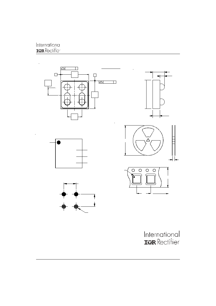
RECOMMENDED FOOTPRINT
0.800 [.032]
Anode Ball 3
Anode Ball 4
0.800 [.032]
Cathode Ball 2
Cathode Ball 1
4X Ø 0.25 [.010]
IR WORLD HEADQUARTERS: 233 Kansas St., El Segundo, California 90245, USA Tel: (310) 252-7105
TAC Fax: (310) 252-7309
Visit us at www.irf.com for sales contact information. 08/05
Data and specifications subject to change without notice.
This product has been designed for Consumer Level.
Qualification Standards can be found on IR's Web site.
0101
0001
DATE CODE
LOT NUMBER
BALL 1 MARK
IR
PART NUMBER
130C
1.524
[.060]
0.800
[.032]
4X
B
1.524
[.060]
A
0.400
[.016]
2X
NOTES:
1. DIMENSIONING & TOLERANCING PER ASME Y14.5M-1994.
2. CONTROLLING DIMENSION: MILLIMETER
3. DIMENSIONS ARE SHOWN IN MILLIMETERS [INCHES].
1
0.10 [.004] C
2X
0.10 [.004] C
2X
2 = CATHODE
3 = ANODE
1 = CATHODE
4 = ANODE
BALL ASSIGNMENTS
2
4
3
8mm
1. TAPE AND REEL OUTLINE CONFORMS TO EIA-481 & EIA-541.
NOTES:
8mm
4mm
FEED DIRECTION
LOCATION
A1 BALL
Ø 13"
FlipKY
TM
Outline Dimension and Tape and Reel
0.355
0.395
1.524
0.675
0.595
0.240
0.280