Äîêóìåíòàöèÿ è îïèñàíèÿ www.docs.chipfind.ru
Features
·
Over temperature shutdown
·
Over current shutdown
·
Active clamp
·
Low current & logic level input
·
E.S.D protection
IPS031R
FULLY PROTECTED POWER MOSFET SWITCH
Data Sheet No.PD60220
Description
The IPS031R are fully protected three terminal SMART
POWER MOSFETs that feature over-current, over-tem-
perature, ESD protection and drain to source active
clamp.These devices combine a HEXFET® POWER
MOSFET and a gate driver. They offer full protection
and high reliability required in harsh environments.
The driver allows short switching times and provides
efficient protection by turning OFF the power MOSFET
when the temperature exceeds 165
o
C or when the
drain current reaches 14A. The device restarts once the
input is cycled. The avalanche capability is significantly
enhanced by the active clamp and covers most induc-
tive load demagnetizations.
Product Summary
R
ds(on)
60m
(max)
V
clamp
50V
I
shutdown
14A
T
on
/T
off
1.5
µ
s
www.irf.com
1
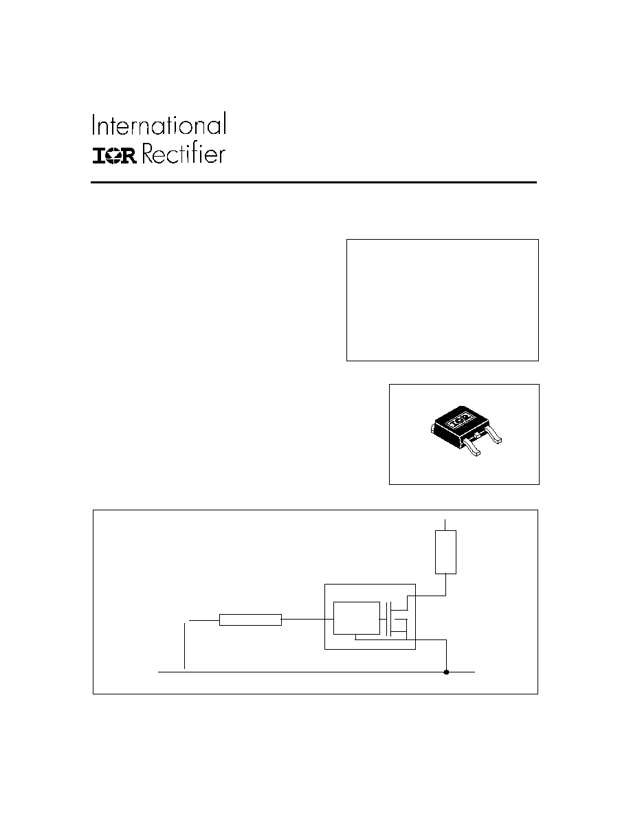
Package
Typical Connection
(Refer to lead assignment for correct pin configuration)
!
!
!
!
!
"
"
"
"
"
Load
D
S
control
IN
R in series
(if needed)
Logic signal
3-Lead D
-
Pak
IPS031R
2
www.irf.com
(1) Limited by junction temperature (pulsed current limited also by internal wiring)
(2) Operations at higher switching frequencies is possible. See Application. Notes.
Recommended Operating Conditions
These values are given for a quick design. For operation outside these conditions, please consult the application notes.
Symbol Parameter
Min.
Max. Units
Vds (max) Continuous drain to source voltage
--
35
VIH
High level input voltage
4
6
VIL
Low level input voltage
0
0.5
Ids
Continuous drain current
Tamb=85
o
C
TAmbient = 85
o
C, IN = 5V, rth = 50
o
C/W, Tj = 125
o
C) 1" sq. footprint
--
3.3
A
TAmbient = 85
o
C, IN = 5V, rth = 100
o
C/W, Tj = 125
o
C) Std. footprint
--
2
Rin
Recommended resistor in series with IN pin
0.2
5
k
Tr-in(max) Max recommended rise time for IN signal (see fig. 2)
--
1
µ
S
Fr-Isc
(2)
Max. frequency in short circuit condition (Vcc = 14V)
0
1
kHz
V
Absolute Maximum Ratings
Absolute maximum ratings indicate sustained limits beyond which damage to the device may occur. All voltage parameters
are referenced to SOURCE lead. (TAmbient = 25
o
C unless otherwise specified). PCB mounting uses the standard foot-
print with 70
µ
m copper thickness.
Symbol Parameter
Min.
Max.
Units
Test Conditions
Vds
Maximum drain to source voltage
--
47
Vin
Maximum input voltage
-0.3
7
Iin, max
Maximum IN current
-10
+10
mA
Isd
cont.
Diode max. continuous current
(1)
rth=100
o
C/W
--
1.6
D-Pak Std footprint
rth=5
o
C/W
--
18
D-Pak with Rth=5
o
C/W
rth=50
o
C/W
-- 3 D-Pak with sq. footprint
Isd
pulsed
Diode max. pulsed current
(1)
--
18
Pd
Maximum power dissipation
(1)
rth=50
o
C/W
--
2.5
rth=100
o
C/W
--
1.25
ESD1
Electrostatic discharge voltage
(Human Body)
--
4
C=100pF, R=1500
,
ESD2
Electrostatic discharge voltage
(Machine Model)
--
0.5
C=200pF, R=0
,
L=10
µ
H
T stor.
Max. storage temperature
-55
150
Tj max.
Max. junction temperature
-40
+150
Tlead
Lead temperature (soldering, 10 seconds)
--
300
V
W
A
o
C
Symbol Parameter
Min.
Typ.
Max. Units Test Conditions
Rth 1
Thermal resistance with standard footprint
--
100
--
Rth 2
Thermal resistance with 1" square footprint
--
50
--
Rth 3
Thermal resistance junction to case
--
3
--
Thermal Characteristics
o
C/W D
-
PAK
kV
IPS031R
www.irf.com
3
Symbol Parameter
Min.
Typ.
Max. Units Test Conditions
Tsd
Over temperature threshold
--
165
--
o
C
See fig. 1
Isd
Over current threshold
10
14
18
A
See fig. 1
V
reset
IN protection reset threshold
1.5
2.3
3
V
Treset
Time to reset protection
2
10 40
µ
s Vin = 0V, Tj = 25
o
C
EOI_OT
Short circuit energy (see application note)
--
400
--
µ
J
Vcc = 14V
Protection Characteristics
Symbol Parameter
Min.
Typ.
Max. Units Test Conditions
Rds(on)
ON state resistance Tj = 25
o
C
20
45
60
Rds(on)
ON state resistance Tj = 150
o
C
--
75
100
Idss
Drain to source leakage current
0
0.5
25
Vcc = 14V, Tj = 25
o
C
@Tj=25
o
C
Idss2
Drain to source leakage current
0
5
50
Vcc = 40V, Tj = 25
o
C
@Tj=25
o
C
V
clamp 1
Drain to source clamp voltage 1
47
52
56
Id = 20mA
(see Fig.3 & 4)
V
clamp 2
Drain to source clamp voltage 2
50
53
60
Vin
clamp
IN to source clamp voltage
7
8.1
9.5
Iin = 1 mA
Vth
IN threshold voltage
1
1.6
2
Id = 50mA, Vds = 14V
Iin, -on
ON state IN positive current
25
90
200
Vin = 5V
Iin, -off
OFF state IN positive current
50
130
250
Vin = 5V
over-current triggered
Static Electrical Characteristics
(Tj = 25
o
C unless otherwise specified.)
m
Vin = 5V, Ids = 1A
Id=Ishutdown
(see Fig.3 & 4)
V
Switching Electrical Characteristics
Vcc = 14V, Resistive Load = 5
, Rinput = 50
,
100
µ
s pulse,T
j
= 25
o
C, (unless otherwise specified).
Symbol Parameter
Min.
Typ.
Max. Units Test Conditions
Ton
Turn-on delay time
0.05
0.3
0.6
Tr
Rise time
0.4
1
2
Trf
Time to 130% final Rds(on)
--
8
--
Toff
Turn-off delay time
0.8
2
3.5
Tf
Fall time
0.5
1.5
2.5
Qin
Total gate charge
--
11
--
nC
Vin = 5V
See figure 2
See figure 2
µ
s
µ
A
µ
A
IPS031R
4
www.irf.com
Lead Assignments
IN
DRAIN
SOURCE
8.1 V
80
µ
A
47 V
I sense
200 k
300
S
Q
R
Q
T > 165°c
I > 1sd
Functional Block Diagram
All values are typical
D-Pak
IPS031R
1 3
In D S
2 (D)
IPS031R
www.irf.com
5
14 V
IN
D
S
5 v
0 v
L
R
+
-
Vds
Ids
Vin
V load
Rem : V load is negative
during demagnetization
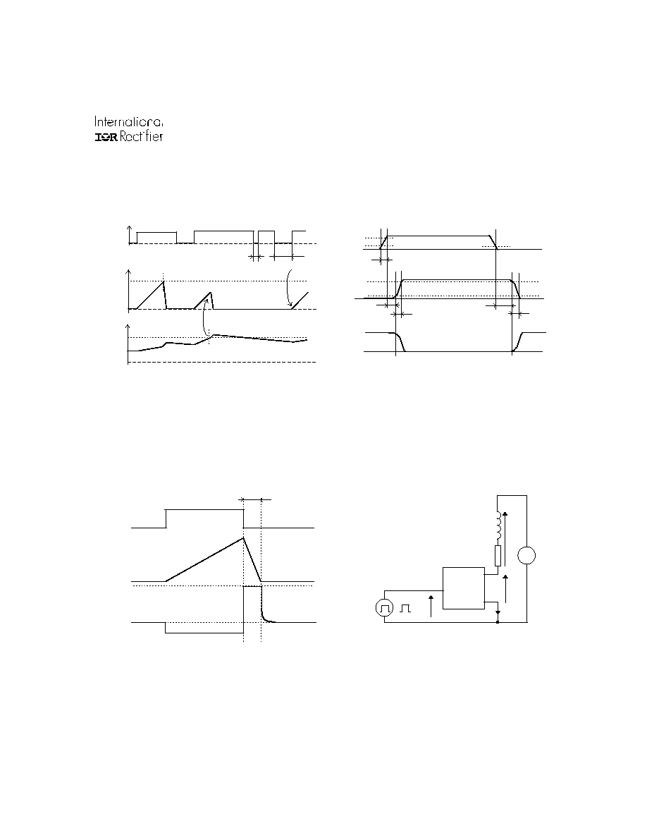
Figure 4 - Active clamp test circuit
Ids
Vds
Vin
T clamp
Vds clamp
( Vcc )
( see Appl . Notes to evaluate power dissipation )
Figure 3 - Active clamp waveforms
Figure 1 - Timing diagram
Tr-in
10 %
90 %
90 %
10 %
Td on
Td off
tf
tr
Ids
Tr-in
Vin
Vds
Figure 2 - IN rise time & switching time definitions
Tsd
(165 °c)
Vin
Ids
Isd
I shutdown
T
T shutdown
t < T reset
t > T reset
5 V
0 V
IPS031R
6
www.irf.com
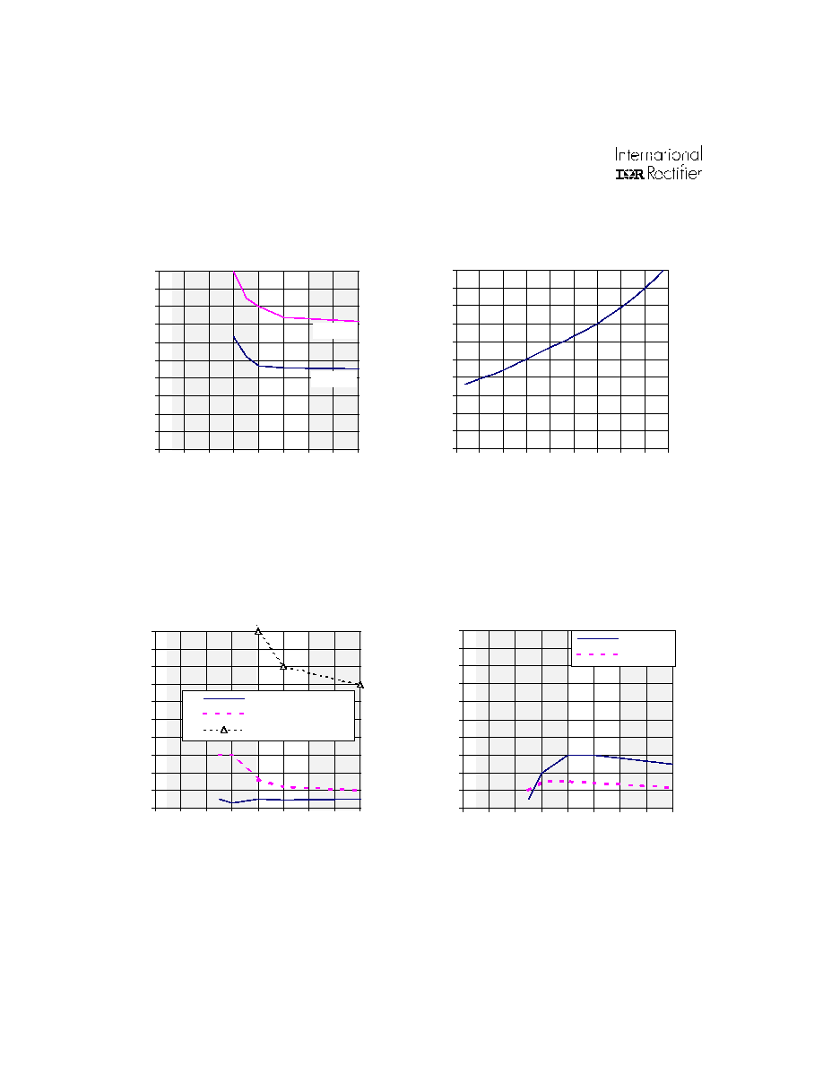
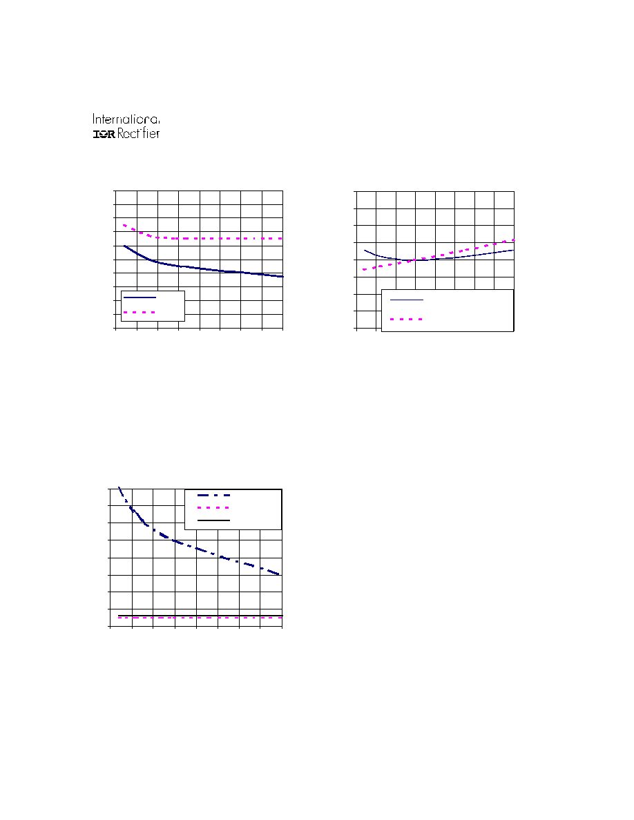
Figure 6 - Normalised Rds ON (%) Vs Tj (
o
C)
Figure 8 - Turn-OFF Delay Time & Fall Time (us)
Vs Input Voltage (V)
Figure 7 - Turn-ON Delay Time, Rise Time & Time
to 130% final Rds(on) (us) Vs Input Voltage (V)
Figure 5 - Rds ON (m
) Vs Input Voltage (V)
All curves are typical values with standard footprints. Operating in the shaded area is not recommended.
0
1
2
3
4
5
6
7
8
9
10
0
1
2
3
4
5
6
7
8
ton delay
rise tim e
130% final rdson
0
10
20
30
40
50
60
70
80
90
100
0
1
2
3
4
5
6
7
8
Tj = 150
o
C
Tj = 25
o
C
0
1
2
3
4
5
6
7
8
9
10
0
1
2
3
4
5
6
7
8
toff delay
fall time
0%
20%
40%
60%
80%
100%
120%
140%
160%
180%
200%
-50 -25
0
25 50 75 100 125 150 175
IPS031R
www.irf.com
7
Figure 12 - I shutdown (A) Vs Temperature (
o
C)
Figure 9 - Turn-ON Delay Time, Rise Time & Time
to 130% final Rds(on) (us) Vs IN Resistor (
)
Figure 10 - Turn-OFF Delay Time & Fall
Time (us) Vs IN Resistor (
)
Figure 11 - Current Iimitation & I shutdown (A)
Vs Vin (V)
0 .1
1
1 0
1 0 0
10
100
1000
10000
delay on
rise time
130% rdson
0 .1
1
1 0
1 0 0
1 0
1 0 0
1 0 0 0
1 0 0 0 0
delay off
fall time
0
2
4
6
8
10
12
14
16
18
20
0
1
2
3
4
5
6
7
8
Isd 25°C
Ilim 25°C
0
2
4
6
8
10
12
14
16
18
20
-50 -25
0
25
50 75 100 125 150
IPS031R
8
www.irf.com
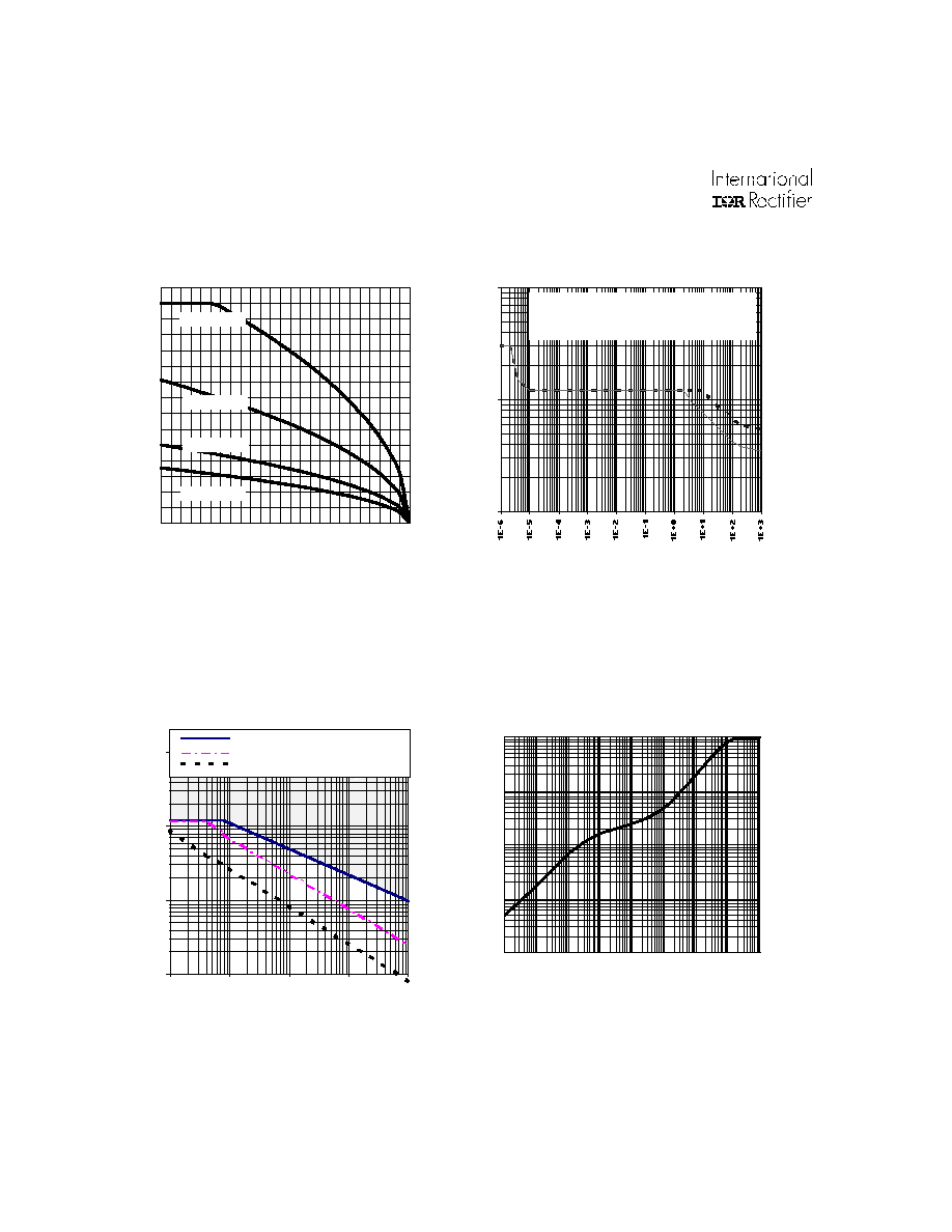
Fig.16 - Transient Thermal Impedance (
o
C/W)
Vs Time (s) - IPS031R
Figure 14 - Ids (A) Vs Protection Resp. Time (s)
IPS031R
Figure 13 - Max. I load current (A) Vs Tamb (
o
C)
IPS031R
Figure 15 - Iclamp (A) Vs Inductive Load (mH)
1
10
100
- - - - Tj=25 °C _____Tj = 100 °C
Free air / standard footprint
0
5
10
15
25
50
75
100
125
150
Rthja=5°C/W
Rthja=15°C/W
Rthja=50°C/W
Rthja=100°C/
0.01
0.1
1
10
100
1.E-05
1.E-03
1.E-01
1.E+01
1.E+03
Vbat = 14 V
Tjini = T sd
0.1
1
10
100
0 .0 1
0 .1
1
1 0
1 0 0
single pulse m ax. current
100 Hz rth=60°C/W dT=25°C
1kHz rth=60°C/W dT=25°C
5
5
IPS031R
www.irf.com
9
0
20
40
60
80
100
120
140
160
180
200
-50 -25
0
25
50
75 100 125 150
Iin,on
Iin,off
80%
85%
90%
95%
100%
105%
110%
115%
120%
-50 -25
0
25
50
75 100 125 150
Vds clamp @ Isd
Vin clamp @ 10mA
Figure 18 - Vin clamp and V clamp2 (%)
Vs Tj (
o
C)
Figure 17 - Input current (
µ
A) Vs Junction (
o
C)
0
2
4
6
8
10
12
14
16
-50 -25
0
25
50
75
100 125 150
Treset
rise time
fall time
Figure 19 - Turn-on, Turn-off, and treset (
µ
s)
Vs Tj (
o
C)
IPS031R
10
www.irf.com
3-Lead D-Pak
01-6031 00
01-0003 03 (JEDEC TO252AA)
Case Outline
IPS031R
www.irf.com
11
Tape & Reel - D
-
PAK
IR WORLD HEADQUARTERS: 233 Kansas St., El Segundo, California 90245 Tel: (310) 252-7105
This device was designed and qualified peer automotive level (Q101)
Data and specifications subject to change without notice. 6/1/2004
01-3072 00