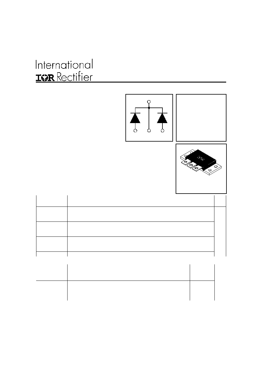
70nk60c
PD -2.460A
Reduced RFI and EMI
Reduced Snubbing
Extensive Characterization of Recovery Parameters
Features
Description
HEXFRED
T M
diodes are optimized to reduce losses and EMI/RFI in high frequency
power conditioning systems. An extensive characterization of the recovery
behavior for different values of current, temperature and di/dt simplifies the
calculations of losses in the operating conditions. The softness of the recovery
eliminates the need for a snubber in most applications. These devices are
ideally suited for power converters, motors drives and other applications where
switching losses are significant portion of the total losses.
Ultrafast, Soft Recovery Diode
HEXFRED
TM
HFA70NK60C
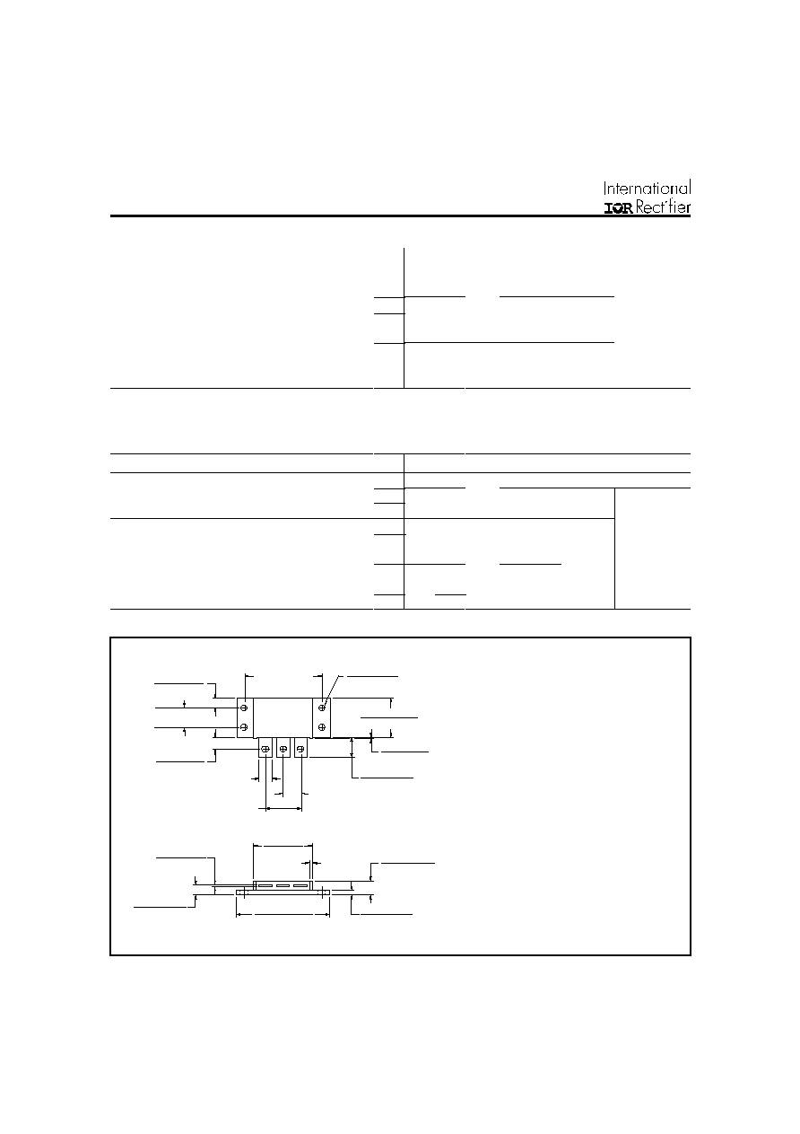
Absolute Maximum Ratings (per Leg)
Note: Limited by junction temperature
L = 100µH, duty cycle limited by max T
J
A
W
°C/W
K/W
Thermal - Mechanical Characteristics
-55 to +150
35 (4.0)
50 (5.7)
Parameter
Max.
Units
V
R
Cathode-to-Anode Voltage
600
V
I
F
@ T
C
= 25°C
Continuous Forward Current
59
I
F
@ T
C
= 100°C
Continuous Forward Current
29
I
FSM
Single Pulse Forward Current
200
I
AS
Maximum Single Pulse Avalanche Current
2.0
E
AS
Non-Repetitive Avalanche Energy
220
µJ
P
D
@ T
C
= 25°C
Maximum Power Dissipation
160
P
D
@ T
C
= 100°C
Maximum Power Dissipation
63
T
J
Operating Junction and
T
STG
Storage Temperature Range
°C
Soldering Temperature, for 10 sec.
300 (0.063 in. (1.6mm) from case)
Parameter
Min.
Typ.
Max.
Units
R
JC
Junction-to-Case, Single Leg Conducting
0.80
Junction-to-Case, Both Legs Conducting
0.40
R
CS
Case-to-Sink, Flat, Greased Surface
0.10
Wt
Weight
58 (2.0)
g (oz)
Mounting Torque
lbfin
See Fig. 12
(Nm)
BASE COMMON CATHODE
3
1
2
COMMON
CATHODE
ANODE
2
ANODE
1
TO-249AA
(MODIFIED)
5/5/97
V
R
= 600V
V
F
(typ.)
= 1.2V
I
F(AV)
= 70A
Q
rr
(typ.) = 210nC
I
RRM
(typ.)
= 6A
t
rr
(typ.)
= 30ns
di
(rec)M
/dt (typ.)
= 180A/µs
125°C
HFA70NK60C
Parameter
Min. Typ. Max. Units
Test Conditions
V
BR
Cathode Anode Breakdown Voltage
600
V
I
R
= 100µA
V
FM
Max Forward Voltage
1.3
1.5
I
F
= 35A
1.5
1.7
V
I
F
= 70A
See Fig. 1
1.2
1.4
I
F
= 35A, T
J
= 125°C
I
RM
Max Reverse Leakage Current
2.0
10
µA
V
R
= V
R
Rated
0.50 2.0
mA
T
J
= 125°C, V
R
= 480V
C
T
Junction Capacitance
68
100
pF
V
R
= 200V
See Fig. 3
L
S
Series Inductance
9.2
nH
Lead to lead 5mm from package body
Electrical Characteristics (per Leg) @ T
J
= 25°C (unless otherwise specified)
Dynamic Recovery Characteristics (per Leg) @ T
J
= 25°C (unless otherwise specified)
A/µs
nC
A
See Fig. 2
Parameter
Min. Typ. Max. Units Test Conditions
t
rr
Reverse Recovery Time
30
I
F
= 1.0A, di
f
/dt = 200A/µs, V
R
= 30V
t
rr1
70
110
ns
T
J
= 25°C
See Fig.
t
rr2
115 180
T
J
= 125°C
5
I
F
= 35A
I
RRM1
Peak Recovery Current
6.0
11
T
J
= 25°C
See Fig.
I
RRM2
9.0
16
T
J
= 125°C
6
V
R
= 200V
Q
rr1
Reverse Recovery Charge
210 580
T
J
= 25°C
See Fig.
Q
rr2
520 1400
T
J
= 125°C
7
di
f
/dt = 200A/µs
di
(rec)M
/dt1
Peak Rate of Fall of Recovery Current
280
T
J
= 25°C
See Fig.
di
(rec)M
/dt2
During t
b
180
T
J
= 125°C
8
Dimensions in millimeters and inches
4.95 (0.195)
61.21 (2.410)
60.71 (2.390)
37.85 (1.490)
38.35 (1.510)
REF.
1.27 (0.050)
3.30 (0.130)
3.05 (0.120)
10.16 (0.400)
8.38 (0.330)
0.89 (0.035)
1.14 (0.045)
6.60 (0.260)
6.10 (0.240)
50.80 (2.000)
REF.
25.65 (1.010)
25.15 (0.990)
12.70 (0.500)
REF.
6.10 (0.240)
6.60 (0.260)
8.05 (0.317)
7.80 (0.307)
0.76 (0.030)
1.14 (0.045)
11.43 (0.450)
REF.
22.86 (0.900)
REF.
DIA.
4.45 (0.175)
(7 PLCS.)
13.21 (0.520)
12.70 (0.500)
8.64 (0.340)
REF. (3 PLCS.)
2
1
3
LEAD ASSIGNMENTS
1 - ANODE
2 - CATHODE
3 - ANODE
BASE COMMON CATHODE
Conforms to JEDEC Outline TO - 249AA (Modified)
See Fig. 1
See Fig. 2
See Fig. 3
See Fig.
5
See Fig.
6
See Fig.
7
See Fig.
8
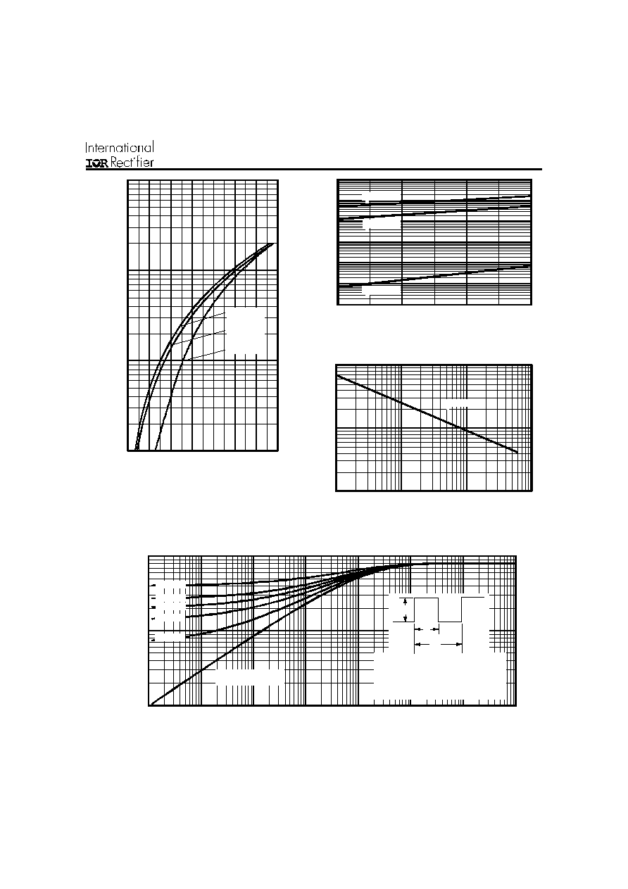
HFA70NK60C
Fig. 4 - Maximum Thermal Impedance Z
thjc
Characteristics, (per Leg)
Fig. 2 - Typical Reverse Current vs. Reverse
Voltage, (per Leg)
Fig. 3 - Typical Junction Capacitance vs.
Reverse Voltage, (per Leg)
Fig. 1 - Maximum Forward Voltage Drop
vs. Instantaneous Forward Current,
(per Leg)
0.01
0.1
1
10
100
1000
10000
0
200
400
600
R
R
Reverse Voltage - V (V)
T = 150°C
Reve
rse Curre
nt - I
(
µA)
T = 125°C
T = 25°C
J
J
J
10
100
1000
1
10
100
1000
T = 25°C
J
Reverse Voltage - V (V)
R
T
Ju
nction
C
a
pacit
ance - C
(pF)
A
1
10
100
1000
0.4
0.8
1.2
1.6
2.0
2.4
2.8
3.2
FM
F
Insta
ntaneo
us Forward
C
u
rrent - I
(A)
Forward Voltage Drop - V (V)
T = 150°C
T = 125°C
T = 25°C
J
J
J
0.01
0.1
1
0.00001
0.0001
0.001
0.01
0.1
1
10
100
1
th
JC
t , Rectangular Pulse Duration (Seconds)
D = 0.50
D = 0.33
D = 0.25
D = 0.17
D = 0.08
Single Pulse
(Thermal Resistance)
T
h
er
m
a
l
I
m
ped
anc
e -
Z
(
K
/
W
)
2
t
1
t
P
DM
Notes:
1. Duty factor D = t / t
2. Peak T = P x Z + T
J
DM
thJC
C
2
1
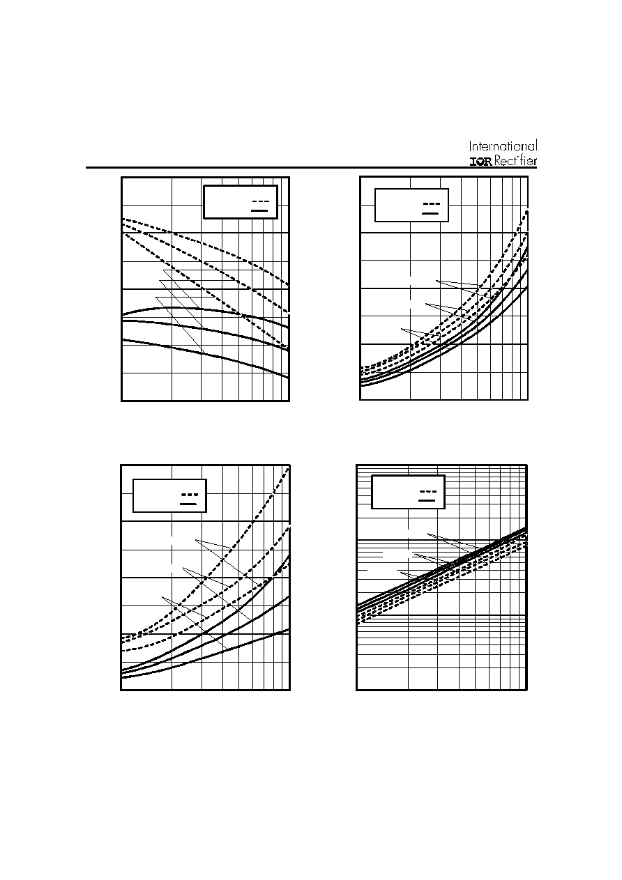
HFA70NK60C
Fig. 7 - Typical Stored Charge vs. di
f
/dt,
(per Leg)
Fig. 8 - Typical di
(rec)M
/dt vs. di
f
/dt,
(per Leg)
Fig. 5 - Typical Reverse Recovery vs. di
f
/dt,
(per Leg)
Fig. 6 - Typical Recovery Current vs. di
f
/dt,
(per Leg)
30
60
90
120
150
100
1000
f
di /dt - (A/µs)
I = 15A
F
t
- (ns)
rr
I = 70A
I = 35A
V = 200V
T = 125°C
T = 25°C
R
J
J
F
F
0
10
20
30
40
100
1000
f
di /dt - (A/µs)
I = 15A
F
t - (ns
)
rr
I = 70A
I = 35A
V = 200V
T = 125°C
T = 25°C
R
J
J
F
F
0
400
800
1200
1600
100
1000
f
di /dt - (A/µs)
RR
Q -
(nC)
I = 15A
F
I = 70A
I = 35A
F
F
V = 200V
T = 125°C
T = 25°C
R
J
J
10
100
1000
10000
100
1000
f
di /dt - (A/µs)
d
i
(rec)M/dt
- (A/
µs)
I = 15A
F
I = 70A
I = 35A
V = 200V
T = 125°C
T = 25°C
R
J
J
F
F
HFA70NK60C
4. Q
rr
- Area under curve defined by t
rr
and I
RRM
t
rr
X I
RRM
Q
rr
=
2
5. di
(rec)M
/dt - Peak rate of change of
current during t
b
portion of t
rr
V
(AVAL)
R(RATED)
I
L(PK)
V
DECAY
TIME
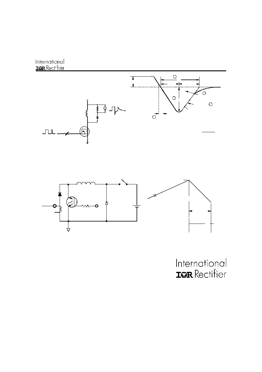
Fig. 11 - Avalanche Test Circuit and Waveforms
Fig. 10 - Reverse Recovery Waveform and
Definitions
Fig. 9 - Reverse Recovery Parameter Test
Circuit
t
a
t
b
t
rr
Q
rr
I
F
I
RRM
I
RRM
0.5
di(rec)M/dt
0.75 I
RRM
5
4
3
2
0
1
di /dt
f
1. di
f
/dt - Rate of change of current
through zero crossing
2. I
RRM
- Peak reverse recovery current
3. trr - Reverse recovery time measured
from zero crossing point of negative
going I
F
to point where a line passing
through 0.75 I
RRM
and 0.50 I
RRM
extrapolated to zero current
REVERSE RECOVERY CIRCUIT
IRFP250
D.U.T.
L = 70µH
V = 200V
R
0.01
G
D
S
dif/dt
ADJUST
CURRENT
MONITOR
HIGH-SPEED
SWITCH
DUT
Rg = 25 ohm
+
FREE-WHEEL
DIODE
Vd = 50V
L = 100µH
WORLD HEADQUARTERS: 233 Kansas St., El Segundo, California 90245, Tel: (310) 322 3331
EUROPEAN HEADQUARTERS: Hurst Green, Oxted, Surrey RH8 9BB, UK Tel: ++ 44 1883 732020
IR CANADA: 7321 Victoria Park Ave., Suite 201, Markham, Ontario L3R 2Z8, Tel: (905) 475 1897
IR GERMANY: Saalburgstrasse 157, 61350 Bad Homburg Tel: ++ 49 6172 96590
IR ITALY: Via Liguria 49, 10071 Borgaro, Torino Tel: ++ 39 11 451 0111
IR FAR EAST: K&H Bldg., 2F, 30-4 Nishi-Ikebukuro 3-Chome, Toshima-Ku, Tokyo Japan 171 Tel: 81 3 3983 0086
IR SOUTHEAST ASIA: 315 Outram Road, #10-02 Tan Boon Liat Building, Singapore 0316 Tel: 65 221 8371
http://www.irf.com/
Data and specifications subject to change without notice.
5/97