
PD -2.459 rev. B 01/99
· Reduced RFI and EMI
· Reduced Snubbing
· Extensive Characterization of
Recovery Parameters
Features
Description
HEXFRED
TM
diodes are optimized to reduce losses and EMI/RFI in high frequency
power conditioning systems. An extensive characterization of the recovery
behavior for different values of current, temperature and di/dt simplifies the
calculations of losses in the operating conditions. The softness of the recovery
eliminates the need for a snubber in most applications. These devices are ideally
suited for power converters, motors drives and other applications where
switching losses are significant portion of the total losses.
Ultrafast, Soft Recovery Diode
HEXFRED
TM
HFA70NC60CSM
Absolute Maximum Ratings (per Leg)
SM D -61-8
Note:
Limited by junction temperature
L = 100µH, duty cycle limited by max T
J
Thermal - Mechanical Characteristics
V
R
= 600V
V
F
(typ.)
= 1.2V
I
F(AV)
= 70A
Q
rr
(typ.) = 210nC
I
RRM
(typ.)
= 6A
t
rr
(typ.)
= 30ns
di
(rec)M
/dt (typ.)
= 180A/µs
125°C
W
Parameter
Max.
Units
V
R
Cathode-to-Anode Voltage
600
V
I
F
@ T
C
= 25°C
Continuous Forward Current
56
I
F
@ T
C
= 100°C
Continuous Forward Current
27
A
I
FSM
Single Pulse Forward Current
200
E
AS
Non-Repetitive Avalanche Energy
220
µJ
P
D
@ T
C
= 25°C
Maximum Power Dissipation
150
P
D
@ T
C
= 100°C
Maximum Power Dissipation
59
T
J
Operating Junction and
T
STG
Storage Temperature Range
Soldering Temperature, for 10 sec.
300 (0.063 in. (1.6mm) from case)
-55 to +150
°C
Parameter
Min.
Typ.
Max.
Units
R
thJC
Junction-to-Case, Single Leg Conducting
0.85
Junction-to-Case, Both Legs Conducting
0.42
Wt
Weight
4.3 (0.15)
g (oz)
°C/W
K/W
1

HFA70NC60CSM
PD-2.459 rev. B 01/99
2
Electrical Characteristics (per Leg) @ T
J
= 25°C (unless otherwise specified)
Dynamic Recovery Characteristics (per Leg) @ T
J
= 25°C (unless otherwise specified)
Parameter
Min. Typ. Max. Units
Test Conditions
V
BR
Cathode Anode Breakdown Voltage
600
V
I
R
= 100µA
V
FM
Max Forward Voltage
1.3
1.5
I
F
= 35A
1.5
1.7
V
I
F
= 70A
1.2
1.4
I
F
= 35A, T
J
= 125°C
I
RM
Max Reverse Leakage Current
2.0
10
µA
V
R
= V
R
Rated
0.50
2.0
mA
T
J
= 125°C, V
R
= 480V
C
T
Junction Capacitance
68
100
pF
V
R
= 200V
L
S
Series Inductance
5.5
nH
Lead to lead 5mm from package body
See Fig. 1
See Fig. 2
See Fig. 3
A/µs
nC
A
Parameter
Min. Typ. Max. Units Test Conditions
t
rr
Reverse Recovery Time
30
I
F
= 1.0A, di
f
/dt = 200A/µs, V
R
= 30V
t
rr1
70
110
ns
T
J
= 25°C
t
rr2
115
180
T
J
= 125°C
I
F
= 35A
I
RRM1
Peak Recovery Current
6.0
11
T
J
= 25°C
I
RRM2
9.0
16
T
J
= 125°C
V
R
= 200V
Q
rr1
Reverse Recovery Charge
210
580
T
J
= 25°C
Q
rr2
520
1400
T
J
= 125°C
di
f
/dt = 200A/µs
di
(rec)M
/dt1
Peak Rate of Fall of Recovery Current
280
T
J
= 25°C
di
(rec)M
/dt2
During t
b
180
T
J
= 125°C
See Fig.
5
See Fig.
6
See Fig.
7
See Fig.
8
Outline D61- 8-SM
Dimensions in millimeters and (inches)

HFA70NC60CSM
PD-2.459 rev. B 01/99
3
Fig. 4 - Maximum Thermal Impedance Z
thjc
Characteristics, (per Leg)
Fig. 2 - Typical Reverse Current vs. Reverse
Voltage, (per Leg)
Fig. 3 - Typical Junction Capacitance vs.
Reverse Voltage, (per Leg)
Fig. 1 - Maximum Forward Voltage Drop
vs. Instantaneous Forward Current,
(per Leg)
0.01
0.1
1
1 0
10 0
100 0
1 00 0 0
0
2 0 0
400
600
R
R
R e v e rse V o lta g e - V (V )
T = 1 5 0 °C
R
e
v
e
rs
e
C
u
rre
n
t
- I
(µ
A
)
T = 1 2 5 °C
T = 2 5 °C
J
J
J
1 0
10 0
1 00 0
1
1 0
1 0 0
1 000
T = 2 5 °C
J
R e ve rs e V o lta g e - V (V )
R
T
J
u
nc
t
i
on
Capa
c
i
t
a
nc
e
-
C
(
p
F
)
A
1
10
100
1000
0.4
0.8
1.2
1.6
2.0
2.4
2.8
3.2
F M
F
I
n
s
t
an
t
a
ne
ous
F
o
r
w
ar
d
Cur
r
e
n
t
-
I
(
A
)
F o rw a rd V o lta g e D ro p - V (V )
T = 1 5 0 °C
T = 1 2 5 °C
T = 2 5 °C
J
J
J
0.01
0.1
1
0.0001
0.001
0.01
0.1
1
10
100
1
th
J
C
t , R e cta n g u la r P u lse D u ra tio n (S e co n d s)
D = 0.50
D = 0.33
D = 0.25
D = 0.1 7
D = 0.08
S in g le P u ls e
(Th e rm a l R e s is ta n c e )
T
h
e
r
m
a
l I
m
p
e
d
a
n
c
e
-
Z
(
K
/
W
)
2
t
1
t
P
D M
N o te s:
1 . D u ty fa cto r D = t / t
2 . P e a k T = P x Z + T
J
D M
th JC
C
2
1

HFA70NC60CSM
PD-2.459 rev. B 01/99
4
Fig. 7 - Typical Stored Charge vs. di
f
/dt,
(per Leg)
Fig. 8 - Typical di
(rec)M
/dt vs. di
f
/dt,
(per Leg)
Fig. 5 - Typical Reverse Recovery vs. di
f
/dt,
(per Leg)
Fig. 6 - Typical Recovery Current vs. di
f
/dt,
(per Leg)
0
1 0
2 0
3 0
4 0
1 0 0
10 0 0
f
d i /d t - (A /µ s)
I = 1 5 A
F
t
-
(
n
s
)
rr
I = 7 0 A
I = 3 5 A
V = 2 0 0 V
T = 1 2 5 °C
T = 2 5 °C
R
J
J
F
F
30
60
90
120
150
1 00
1 000
f
d i /d t - (A /µ s)
I = 1 5 A
F
t
-
(
n
s
)
rr
I = 7 0 A
I = 3 5 A
V = 2 0 0 V
T = 1 2 5 °C
T = 2 5 °C
R
J
J
F
F
0
400
800
1 20 0
1 60 0
100
100 0
f
d i /d t - (A /µ s )
RR
Q
-
(
n
C
)
I = 1 5 A
F
I = 7 0 A
I = 3 5 A
F
F
V = 2 0 0 V
T = 1 2 5 °C
T = 2 5 °C
R
J
J
10
1 00
1 0 0 0
1 0 0 0 0
1 0 0
1 00 0
f
d i /d t - (A /µ s )
d
i
(re
c
)
M
/
d
t
-
(A
/
µ
s
)
I = 1 5 A
F
I = 7 0 A
I = 3 5 A
V = 2 0 0 V
T = 1 2 5 °C
T = 2 5 °C
R
J
J
F
F
HFA70NC60CSM
PD-2.459 rev. B 01/99
5
4. Q
rr
- Area under curve defined by t
rr
and I
RRM
t
rr
X I
RRM
Q
rr
=
2
5. di
(rec)M
/dt - Peak rate of change of
current during t
b
portion of t
rr
V
(A V A L)
R (R A T E D )
I
L(P K )
V
D E C A Y
T IM E
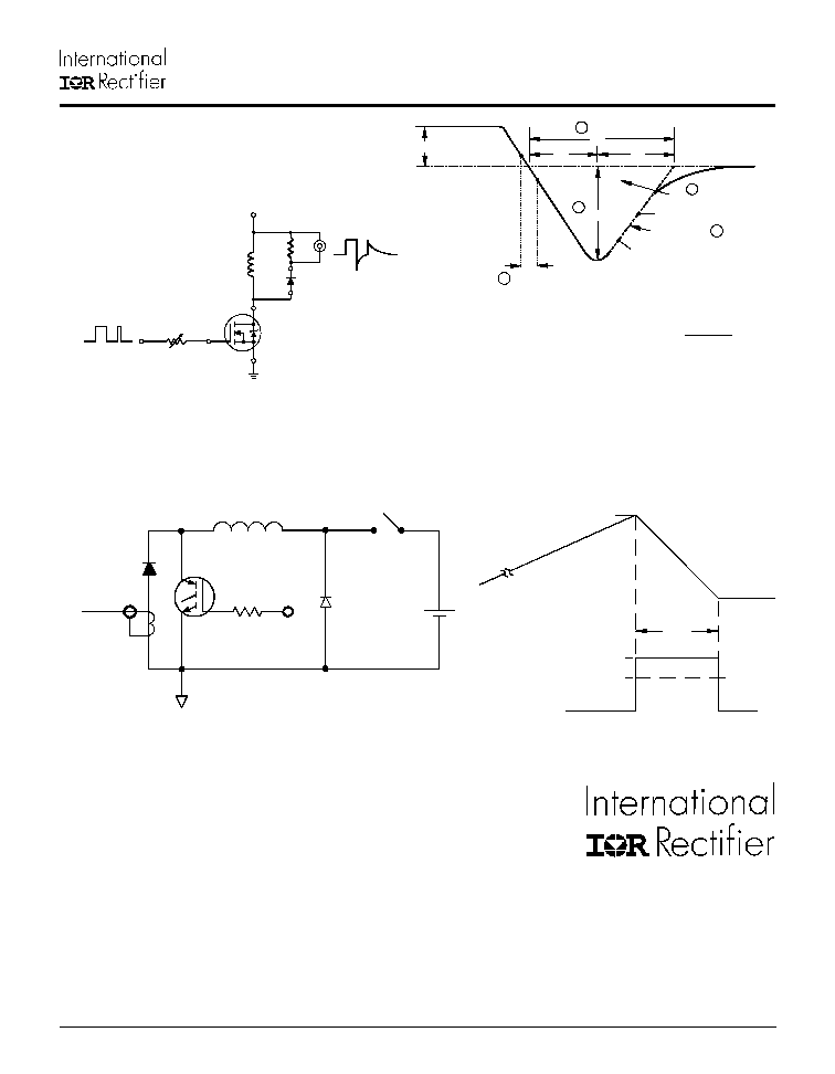
Fig. 11 - Avalanche Test Circuit and Waveforms
Fig. 10 - Reverse Recovery Waveform and
Definitions
Fig. 9 - Reverse Recovery Parameter Test
Circuit
t
a
t
b
t
rr
Q
rr
I
F
I
R R M
I
R R M
0 .5
d i(re c)M /d t
0.75 I
R R M
5
4
3
2
0
1
d i /d t
f
1. di
f
/dt - Rate of change of current
through zero crossing
2. I
RRM
- Peak reverse recovery current
3. trr - Reverse recovery time measured
from zero crossing point of negative
going I
F
to point where a line passing
through 0.75 I
RRM
and 0.50 I
RRM
extrapolated to zero current
R E V E R S E R E C O V E R Y C IR C U IT
IR F P 2 50
D .U .T .
L = 7 0 µ H
V = 2 00 V
R
0.01
G
D
S
d if/d t
A D JU S T
C U R R E N T
M O N IT O R
H IG H -S P E E D
S W IT C H
D U T
R g = 2 5 o h m
+
F R E E -W H E E L
D IO D E
V d = 5 0 V
L = 1 0 0 µ H
http://www.irf.com Fax-On-Demand: +44 1883 733420 Data and specifications subject to change without notice.
233 Kansas St., El Segundo, California 90245 U.S.A. Tel: (310) 322 3331. Fax: (310) 322 3332.
Hurst Green, Oxted, Surrey RH8 9BB, U.K. Tel: ++ 44 1883 732020. Fax: ++ 44 1883 733408.
15 Lincoln Court, Brampton, Markham, Ontario L6T3Z2. Tel: (905) 453 2200. Fax: (905) 475 8801.
Saalburgstrasse 157, 61350 Bad Homburg. Tel: ++ 49 6172 96590. Fax: ++ 49 6172 965933.
Via Liguria 49, 10071 Borgaro, Torino. Tel: ++ 39 11 4510111. Fax: ++ 39 11 4510220.
K&H Bldg., 2F, 30-4 Nishi-Ikebukuro 3-Chome, Toshima-Ku, Tokyo, Japan 171. Tel: 81 3 3983 0086.
1 Kim Seng Promenade, Great World City West Tower,13-11, Singapore 237994. Tel: ++ 65 838 4630.
16 Fl. Suite D.207, Sec. 2, Tun Haw South Road, Taipei, 10673, Taiwan. Tel: 886 2 2377 9936.
WORLD HEADQUARTERS:
WORLD HEADQUARTERS:
WORLD HEADQUARTERS:
WORLD HEADQUARTERS:
WORLD HEADQUARTERS:
EUROPEAN HEADQUARTERS:
EUROPEAN HEADQUARTERS:
EUROPEAN HEADQUARTERS:
EUROPEAN HEADQUARTERS:
EUROPEAN HEADQUARTERS:
IR CANADA:
IR CANADA:
IR CANADA:
IR CANADA:
IR CANADA:
IR GERMANY:
IR GERMANY:
IR GERMANY:
IR GERMANY:
IR GERMANY:
IR ITALY:
IR ITALY:
IR ITALY:
IR ITALY:
IR ITALY:
IR FAR EAST:
IR FAR EAST:
IR FAR EAST:
IR FAR EAST:
IR FAR EAST:
IR SOUTHEAST ASIA:
IR SOUTHEAST ASIA:
IR SOUTHEAST ASIA:
IR SOUTHEAST ASIA:
IR SOUTHEAST ASIA:
IR TAIWAN:
IR TAIWAN:
IR TAIWAN:
IR TAIWAN:
IR TAIWAN: