Äîêóìåíòàöèÿ è îïèñàíèÿ www.docs.chipfind.ru
PD -20602 rev. B 01/2000
Ultrafast, Soft Recovery Diode
HEXFRED
TM
HFA06TB120S.. Series
-55 to +150
°C
1
W
· Ultrafast Recovery
· Ultrasoft Recovery
· Very Low I
RRM
· Very Low Q
rr
· Guaranteed Avalanche
· Specified at Operating Conditions
Benefits
· Reduced RFI and EMI
· Reduced Power Loss in Diode and Switching
Transistor
· Higher Frequency Operation
· Reduced Snubbing
· Reduced Parts Count
Features
Description
International Rectifier's HFA06TB120S is a state of the art ultra fast recovery diode.
Employing the latest in epitaxial construction and advanced processing techniques it
features a superb combination of characteristics which result in performance which is
unsurpassed by any rectifier previously available. With basic ratings of 1200 volts and 6
amps continuous current, the HFA06TB120S is especially well suited for use as the
companion diode for IGBTs and MOSFETs. In addition to ultra fast recovery time, the
HEXFRED product line features extremely low values of peak recovery current (I
RRM
) and
does not exhibit any tendency to "snap-off" during the t
b
portion of recovery. The
HEXFRED features combine to offer designers a rectifier with lower noise and significantly
lower switching losses in both the diode and the switching transistor. These HEXFRED
advantages can help to significantly reduce snubbing, component count and heatsink
sizes. The HEXFRED HFA06TB120S is ideally suited for applications in power supplies
and power conversion systems (such as inverters), motor drives, and many other similar
applications where high speed, high efficiency is needed.
V
R
= 1200V
V
F
(typ.)* = 2.4V
I
F(AV)
= 6.0A
Q
rr
(typ.)= 116nC
I
RRM
(typ.)
= 4.4A
t
rr
(typ.)
= 26ns
di
(rec)M
/dt (typ.)* = 100A/µs
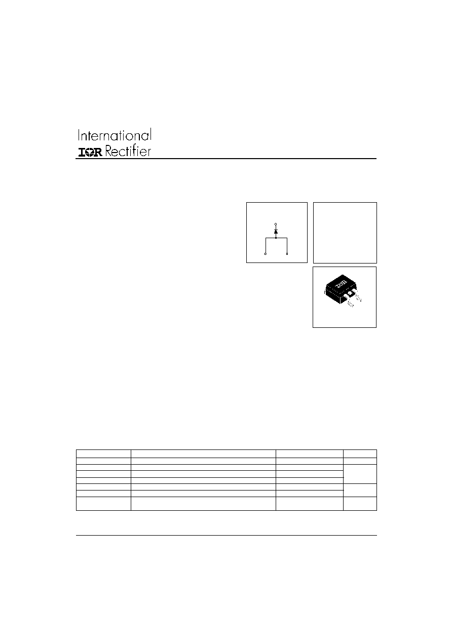
D
2
Pak
1
+
3
2
BASE
(N/C)
(A)
(K)
_
Parameter
Max.
Units
V
R
Cathode-to-Anode Voltage
1200
V
I
F
@ T
C
= 100°C
Continuous Forward Current
8.0
I
FSM
Single Pulse Forward Current
80
A
I
FRM
Maximum Repetitive Forward Current
24
P
D
@ T
C
= 25°C
Maximum Power Dissipation
62.5
P
D
@ T
C
= 100°C
Maximum Power Dissipation
25
T
J
Operating Junction and
T
STG
Storage Temperature Range
Absolute Maximum Ratings
*
125°C

HFA06TB120S..Ser ies
PD-20602 rev. B 01/2000
2
Electrical Characteristics @ T
J
= 25°C (unless otherwise specified)
Thermal - Mechanical Characteristics
Q 0.063 in. from Case (1.6mm) for 10 sec
R Typical Socket Mount
Dynamic Recovery Characteristics @ T
J
= 25°C (unless otherwise specified)
Parameter
Min.
Typ.
Max.
Units
T
lead
Lead Temperature
300
°C
R
thJC
Thermal Resistance, Junction to Case
2.0
R
thJA
Thermal Resistance, Junction to Ambient
80
K/W
R
thCS
Thermal Resistance, Case to Heat Sink
0.5
Wt
Weight
2.0
g
0.07
(oz)
Parameter
Min. Typ. Max. Units Test Conditions
t
rr
Reverse Recovery Time
26
I
F
= 1.0A, di
f
/dt = 200A/µs, V
R
= 30V
t
rr1
53
80
ns
T
J
= 25°C
t
rr2
87
130
T
J
= 125°C
I
F
= 6.0A
I
RRM1
Peak Recovery Current
4.4
8.0
T
J
= 25°C
I
RRM2
5.0
9.0
T
J
= 125°C
V
R
= 200V
Q
rr1
Reverse Recovery Charge
116
320
T
J
= 25°C
Q
rr2
233
585
T
J
= 125°C
di
f
/dt = 200A/µs
di
(rec)M
/dt1 Peak Rate of Recovery
180
T
J
= 25°C
di
(rec)M
/dt2 Current During t
b
100
T
J
= 125°C
R
S
Q
µA
A
nC
A/µs
Parameter
Min. Typ. Max. Units
Test Conditions
V
BR
Cathode Anode Breakdown
1200
V
I
R
= 100µA
Voltage
V
FM
Max. Forward Voltage
2.7
3.0
I
F
= 6.0A
3.5
3.9
V
I
F
= 12A
2.4
2.8
I
F
= 6.0A, T
J
= 125°C
I
RM
Max. Reverse Leakage Current
0.26
5.0
V
R
= V
R
Rated
110
500
T
J
= 125°C, V
R
= 0.8 x V
R
Rated
D
R
C
T
Junction Capacitance
9.0
14
pF
V
R
= 200V
Rated
L
S
Series Inductance
8.0
nH
Measured lead to lead 5mm from pkg body
3
PD-20602 rev. B 01/2000
HFA06TB120S ..Series
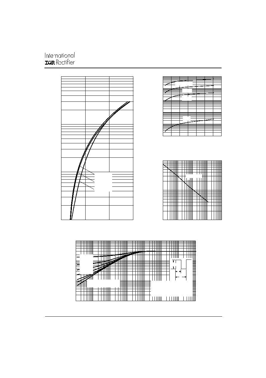
Fig. 1 - Typical Forward Voltage Drop Characteristics
Forward Voltage Drop - V
FM
(V)
Instantaneous Forward Current - I
F
(A)
Reverse Current - I
R
(µ
A)
Reverse Voltage - V
R
(V)
Reverse Voltage - V
R
(V)
Junction Capacitance - C
T
(pF)
Thermal Impedance Z
thJC
(
°
C/W)
Fig. 3 - Typical Junction Capacitance
Vs. Reverse Voltage
0.1
1
10
100
0
2
4
6
T = 150°C
T = 125°C
T = 25°C
J
J
J
0.01
0.1
1
10
0.00001
0.0001
0.001
0.01
0.1
1
10
100
Single Pulse
(Thermal Resistance)
D = 0.50
D = 0.20
D = 0.10
D = 0.05
D = 0.02
D = 0.01
2
t
1
t
P
DM
Notes:
1. Duty factor D = t / t
2. Peak T = P x Z + T
J
DM
thJC
C
2
1
Fig. 4 - Maximum Thermal Impedance ZthJC Characteristics
0.01
0.1
1
10
100
1000
0
200 400 600 800 1000 1200 1400
125°C
100°C
25°C
T = 150°C
J
1
10
100
1
10
100
1000
10000
T = 25°C
J
HFA06TB120S..Ser ies
PD-20602 rev. B 01/2000
4
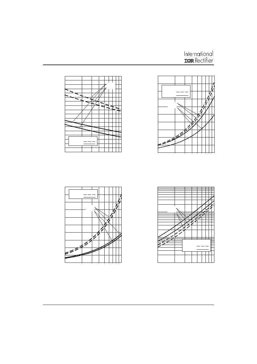
Fig. 5 - Typical Reverse Recovery
Vs. di
f
/dt
Fig. 8 - Typical Stored Charge vs. di
f
/dt
Fig. 6 - Typical Recovery Current
Vs. di
f
/dt
Fig. 7 - Typical di
(REC)
M/dt vs. di
f
/dt
Qrr - ( nC )
di
f
/dt - (A/µs )
di
f
/dt - (A/µs )
20
30
40
50
60
70
80
90
100
110
100
1000
I
F
= 6 A
I
F
= 4 A
R
J
J
V = 200V
T = 125°C
T = 25°C
0
200
400
600
800
1000
100
1000
I
F
= 6 A
I
F
= 4 A
R
J
J
V = 200V
T = 125°C
T = 25°C
trr - ( nC )
Irr - ( A)
di
(REC)
M/dt - (A/µs )
di
f
/dt - (A/µs )
di
f
/dt - (A/µs )
0
5
10
15
20
25
100
1000
I
F
= 6 A
I
F
= 4 A
R
J
J
V = 200V
T = 125°C
T = 25°C
10
100
1000
10000
100
1000
I
F
= 6 A
I
F
= 4 A
R
J
J
V = 200V
T = 125°C
T = 25°C
5
PD-20602 rev. B 01/2000
HFA06TB120S ..Series
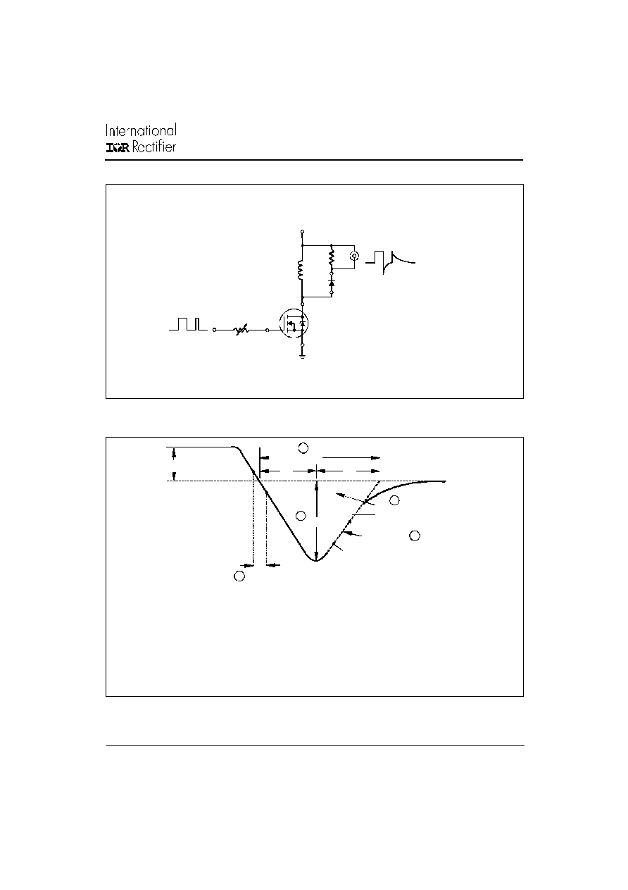
t
a
t
b
t
r r
Q
r r
I
F
I
R R M
I
R R M
0 .5
d i(r e c )M /d t
0 .7 5 I
R R M
5
4
3
2
0
1
d i /d t
f
Fig. 10 - Reverse Recovery Waveform and Definitions
Fig. 9- Reverse Recovery Parameter Test Circuit
R E V E R S E R E C O V E R Y C I R C U IT
IR F P 2 5 0
D .U .T .
L = 7 0 µ H
V = 2 0 0 V
R
0 .0 1
G
D
S
d if/d t
A D J U S T
4. Q
rr
- Area under curve
defined by t
rr
and I
RRM
t
rr
X I
RRM
Q
rr
=
2
5. di
(rec)M
/dt - Peak rate of
change of current during t
b
portion of t
rr
1. di
f
/dt - Rate of change of
current through zero
crossing
2. I
RRM
- Peak reverse
recovery current
3. trr - Reverse recovery
time measured from zero
crossing point of negative
going I
F
to point where a line
passing through 0.75 I
RRM
and 0.50 I
RRM
extrapolated to zero current