Äîêóìåíòàöèÿ è îïèñàíèÿ www.docs.chipfind.ru
40 A
THREE PHASE CONTROLLED BRIDGE
Bulletin I27600 rev. C 11/00
1
45MT160P
Power Module
I
O
40 (36)
A
@ T
C
78 (85)
°C
I
FSM
@ 50Hz
390
A
@ 60Hz
410
I
2
t
@ 50Hz
770
A
2
s
@ 60Hz
700
I
2
t
7700
A
2
s
V
RRM
1600
V
T
STG
range
- 40 to 150
°C
T
J
range
Diode
- 40 to 125
T
J
range
Scr
- 40 to 100
Major Ratings and Characteristics
Features
High thermal conductivity package, electrically insulated case
4000 V
RMS
isolating voltage
Parameters
45MT160P
Units
45MT160P
2
Bulletin I27600 rev. C 11/00
I
O
Maximum DC output current
40 (36)
A
120° Rect conduction angle
@ Case temperature
78 (85)
°C
I
TSM
Maximum peak, one-cycle
390
A
t = 10ms
No voltage
forward, non-repetitive
410
t = 8.3ms reapplied
on state surge current
330
t = 10ms
100% V
RRM
345
t = 8.3ms reapplied
Initial
I
2
t
Maximum I
2
t for fusing
770
A
2
s
t = 10ms
No voltage
T
J
= T
J
max.
700
t = 8.3ms reapplied
540
t = 10ms
100% V
RRM
500
t = 8.3ms reapplied
I
2
t
Maximum I
2
t for fusing
7700
A
2
s
t = 0.1 to 10ms, no voltage reapplied
V
T(TO)
Value of threshold voltage
0.98
V
@ T
J
max.
r
t
Low level value on-state
11
m
V
TM
Maximum on-state voltage drop
1.33
V
I
pk
= 30A, T
J
= 25°C
t
p
= 400µs single junction
di/dt
Maximum non-repetitive rate
150
A/µs
T
J
= 25
o
C, from 0.67 V
DRM
, I
TM
=
x I
T(AV)
,
of rise of turned on current
I
g
= 500mA, t
r
< 0.5 µs, t
p
> 6 µs
I
H
Maximum Holding Current
200
mA
T
J
= 25
o
C, anode supply = 6V,
resistive load, gate open circuit
I
L
Maximum Latching Current
400
T
J
= 25
o
C, anode supply = 6V, resistive load
Forward Conduction
V
INS
RMS isolation voltage
4000
V
T
J
= 25
o
C all terminal shorted
f = 50Hz, t = 1s
dv/dt Max. critical rate of rise
1000
V/µs
T
J
= T
J
max., linear to 0.67 V
DRM
,
of off-state voltage
gate open circuit
Blocking
Voltage
V
RRM
, maximum
V
RSM
, maximum
V
DRM
, max. repetitive
I
RRM
/I
DRM
max.
Type number
Code
repetitive peak
non-repetitive peak
peak off-state voltage
@ T
J
= T
J
max.
reverse voltage
reverse voltage
gate open circuit
V
V
V
mA
45MT160P
160
1600
1700
1600
15
ELECTRICAL SPECIFICATIONS
Voltage Ratings
Parameter
45MT160P
Units Conditions
Parameter
45MT160P
Units Conditions
45MT160P
3
Bulletin I27600 rev. C 11/00
Triggering
P
GM
Max. peak gate power
10
W
T
J
= T
J
max.
P
G(AV)
Max. average gate power
2.5
I
GM
Max. peak gate current
2.5
A
-V
GT
Max. peak negative gate voltage
10
V
V
GT
Max. required DC gate
4.0
V
T
J
= - 40°C
voltage to trigger
2.5
T
J
= 25°C
Anode supply = 6V, resistive load
1.7
T
J
= T
J
max.
I
GT
Max. required DC gate
270
T
J
= - 40°C
current to trigger
150
mA
T
J
= 25°C
Anode supply = 6V, resistive load
80
T
J
= T
J
max.
V
GD
Max. gate voltage
0.25
V
@ T
J
= T
J
max., rated V
DRM
applied
that will not trigger
I
GD
Max. gate current
6
mA
that will not trigger
Thermal and Mechanical Specifications
T
J
Maximum junction operating
- 40 to 125
°C
for diodes
temperature range
- 40 to 100
for Scr
T
stg
Maximum storage temperature
-40 to 150
°C
range
R
thJC
Maximum thermal resistance,
0.32
K/W
DC operation per module
junction to case
1.9
DC operation per junction
0.4
120° Rect condunction angle per module
2.42
120° Rect condunction angle per junction
R
thCS
Maximum thermal resistance,
0.1
K/W
Per module
case to heatsink
Mounting surface smooth, flat an greased
T
Mounting torque ± 10%
4
N m
to heatsink
wt
Approximate weight
60
g
A mounting compound is recommended and the
torque should be rechecked after a period of 3
hours to allow for the spread of the compound.
Lubricated threads.
Parameter
45MT160P
Units Conditions
Parameter
45MT160P
Units Conditions
R Conduction (per Junction)
(The following table shows the increment of thermal resistance R
thJC
when device operate at different conduction angles than DC)
Sinusoidal conduction @ T
J
max.
Rectangular conduction @ T
J
max.
Device
Units
180
o
120
o
90
o
60
o
30
o
180
o
120
o
90
o
60
o
30
o
45MT160P
0.469
0.55
0.69
1.005
1.87
0.289
0.521
0.72
1.065
1.891
K/W
45MT160P
4
Bulletin I27600 rev. C 11/00
1
2
3
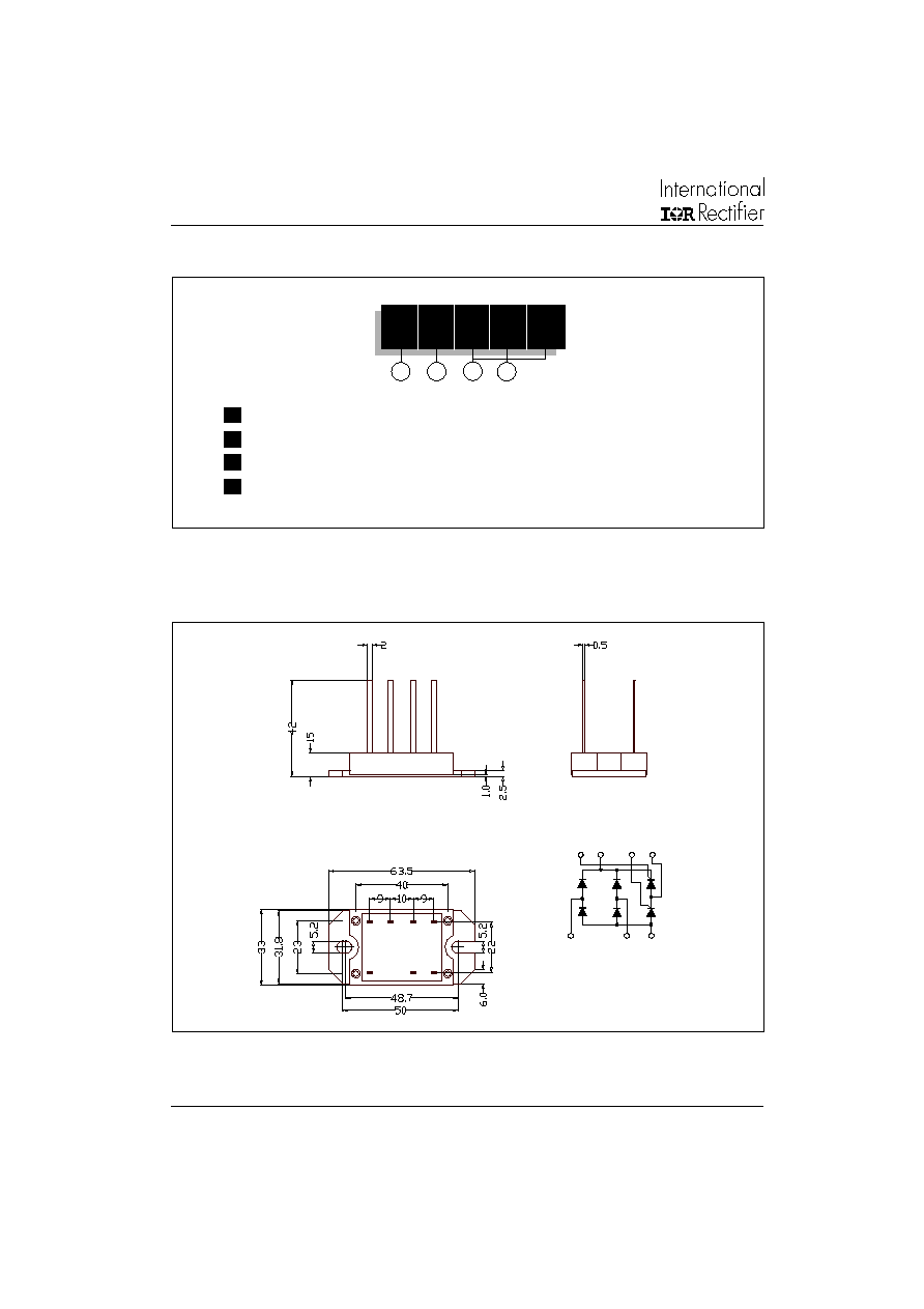
1
- Current rating code: 4 = 40 A (Avg)
2
- Circuit configuration code
3
- Essential part number
4
- Voltage code: Code x 10 = V
RRM
(See Voltage Ratings Table)
4
Device Code
Ordering Information Table
4
5
MT 160
P
Outline Table
All dimensions are in millimeters
1
2
3
4
5
7
8
45MT160P
5
Bulletin I27600 rev. C 11/00
0
20
40
6 0
8 0
1 0 0
1 2 0
14 0
M a xim um A llow a ble A m b ie n t Te m p e ra ture ( C )
10 K/W
5 K /W
3 K/W
2 K
/W
1 .5
K /W
1 K
/W
R
=
0
.7
K /
W
- D
elt
a
R
th
SA
1
1 0
10 0
1 00 0
0
2
4
6
8
10
12
T = 25 C
J
I
n
s
t
a
n
tan
e
ou
s
O
n
-
s
tate
C
u
rr
e
n
t
(
A
)
In stan tan e ous O n -sta te V olta g e (V )
T = 12 5 C
J
16 0
18 0
20 0
22 0
24 0
26 0
28 0
30 0
32 0
34 0
36 0
1
1 0
1 0 0
N um b e r O f E q ua l A m p litud e H a lf C yc le C urre nt P ulses (N )
Pe
a
k
H
a
l
f
S
i
n
e
W
a
ve
On
-
s
t
a
t
e
C
u
r
r
e
n
t
(
A
)
Pe r Jun ction
In itia l T = 125 C
@ 60 Hz 0.0083 s
@ 50 Hz 0.0100 s
J
A t A ny Ra ted Lo a d C o nd itio n A n d W ith
Ra te d V A pp lie d Fo llow ing Surg e .
RRM
1 6 0
1 8 0
2 0 0
2 2 0
2 4 0
2 6 0
2 8 0
3 0 0
3 2 0
3 4 0
3 6 0
3 8 0
4 0 0
0.0 1
0.1
1
P
e
a
k
H
a
l
f
S
i
n
e
W
a
v
e
O
n
-
s
t
a
te
C
u
r
r
e
n
t
(
A
)
Pu lse Tra in D uration (s)
M a xim u m N o n R epe titive Su rg e C u rrent
V ersus Pu lse Tra in D u ra tion . C o n tro l
O f C o nd u ction M a y N ot Be M a inta ine d.
Pe r Ju nctio n
In itia l T = 125 C
N o V o lta ge Re a p p lie d
Ra te d V Rea p p lie d
RRM
J
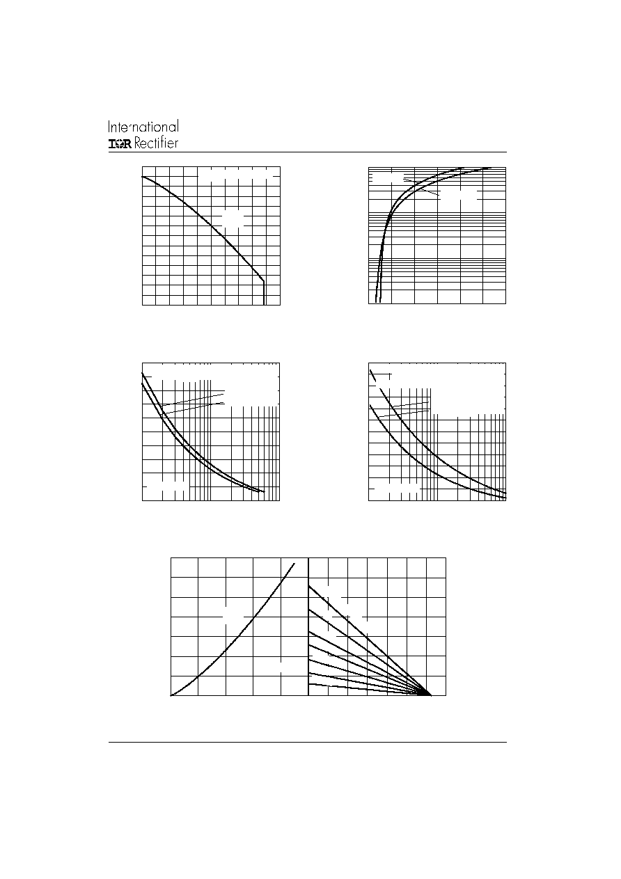
Fig. 1 - Current Rating Characteristics
Fig. 2 - On-state Voltage Drop Characteristics
6 0
7 0
8 0
9 0
1 0 0
1 1 0
1 2 0
1 3 0
0
10
20
3 0
40
5 0
M
a
x
i
m
u
m A
l
l
o
wa
b
l
e
C
a
s
e
T
e
mp
e
r
a
t
u
r
e
(
C
)
Total O utput C urre n t (A )
120
(Re ct)
R (D C ) = 0.32 K/W
thJ C
Fig. 3 - Maximum Non-Repetitive Surge Current
Fig. 4 - Maximum Non-Repetitive Surge Current
0
20
40
60
80
10 0
12 0
14 0
0
10
20
3 0
4 0
5 0
Tota l O utput C urre n t (A )
Ma
x
i
mu
m T
o
t
a
l
P
o
we
r
L
o
s
s
(
W
)
120
(Re ct)
T = 125 C
J
Fig. 5 - Current Rating Nomogram (1 Module Per Heatsink)