1
Ū
FN8145.0
CAUTION: These devices are sensitive to electrostatic discharge; follow proper IC Handling Procedures.
1-888-INTERSIL or 1-888-352-6832
|
Intersil (and design) is a registered trademark of Intersil Americas Inc.
Copyright Intersil Americas Inc. 2005. All Rights Reserved
All other trademarks mentioned are the property of their respective owners.
X60008E-50
Precision 5.0V FGATM Voltage Reference
FEATURES
· Output Voltage: 5.000V
· Absolute Initial Accuracy = ą5mV
· Ultra Low Power Supply Current: 500nA
· Low Temperature Coefficient = 20ppm/°C max
· 10 mA Source & Sink Current Capability
· 10 ppm/1000hrs Long Term Stability
· Very Low Dropout Voltage: 100 mV @ no load
· Supply Voltage Range: 5.1V to 9.0V
· 5kV ESD (Human Body Model)
· Standard Package: SOIC-8
· Temp Range: -40°C to +85°C
DESCRIPTION
The X60008-50 FGATM voltage references are very
high precision analog voltage references fabricated in
Intersil's proprietary Floating Gate Analog technology,
which achieves superior levels of performance when
compared to conventional band gap, buried zener, or
X
FET
TM technologies.
FGATM voltage references feature very high initial
accuracy, very low temperature coefficient, excellent
long term stability, low noise and excellent line and
load regulation, at the lowest power consumption
currently available. These voltage references enable
advanced applications for precision industrial &
portable systems operating at significantly higher
accuracy and lower power levels than can be achieved
with conventional technologies.
APPLICATIONS
· High Resolution A/Ds & D/As
· Precision Current Sources
· Smart sensors
· Digital Meters
· Precision Regulators
· Strain Gage Bridges
· Calibration Systems
· Precision Oscillators
· Threshold Detectors
· V-F Converters
· Battery Management Systems
· Servo Systems
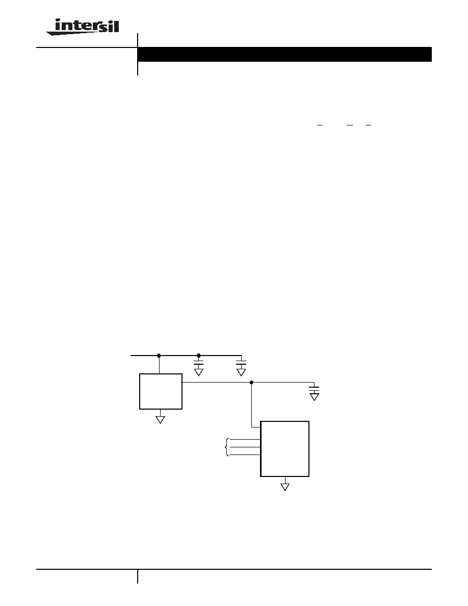
TYPICAL APPLICATION
V
IN
= +6.5V
0.1ĩF
Serial
Bus
V
IN
V
OUT
GND
X60008-50
Enable
SCK
SDAT
A/D Converter
16 to 24-bit
REF IN
10ĩF
0.001ĩF
(
*
)
(
*
)
Also see Figure 3 in Applications Information
Data Sheet
March 14, 2005
2
FN8145.0
March 14, 2005
PACKAGE DIAGRAM
PIN CONFIGURATIONS
ORDERING INFORMATION
Pin Name
Description
GND
Ground Connection
V
IN
Power Supply Input Connection
V
OUT
Voltage Reference Output Connection
DNC
Do Not Connect; Internal Connection Must Be Left Floating
1
2
3
4
8
7
6
5
SOIC
V
IN
DNC
GND
X60008-XX
DNC
DNC
V
OUT
DNC
GND
Logo
Device Part Number
60008 = Standard
Grade
E = ą5.0mV, 20 ppm/°C
Temperature Range
I = -40°C to +85°C
Package
S8 = 8 lead SOIC
V
OUT
Option
50 = 5.000V
X 60008 E I S8 50
X60008E-50
3
FN8145.0
March 14, 2005
ABSOLUTE MAXIMUM RATINGS
Storage Temperature Range............ -65°C to + 125°C
Voltage on any Pin
Referenced to Gnd.............................-0.5V to + 10V
Voltage on "DNC" pins.........No connections permitted
to these pins.
Lead Temperature (soldering, 10 secs).......... + 225°C
RECOMMENDED OPERATING CONDITIONS
COMMENT
Absolute Maximum Ratings indicate limits beyond
which permanent damage to the device and impaired
reliability may occur. These are stress ratings provided
for information only and functional operation of the
device at these or any other conditions beyond those
indicated in the operational sections of this specifica-
tion are not implied.
For guaranteed specifications and test conditions, see
Electrical Characteristics.
The guaranteed specifications apply only for the test
conditions listed. Some performance characteristics
may degrade when the device is not operated under
the listed test conditions.
ELECTRICAL CHARACTERISTICS
(Operating Conditions: V
IN
= 6.5V, I
OUT
= 0mA, C
OUT
= 0.001ĩF, T
A
= -40 to +85°C unless otherwise specified.)
Note:
1. Over the specified temperature range. Temperature coefficient is measured by the box method whereby the change in V
OUT
is divided
by the temperature range; in this case, -40°C to +85°C = 125°C.
2. Thermal Hysteresis is the change in V
OUT
created by package stress @ T
A
= 25°C after temperature cycling. V
OUT
is read initially at T
A
= 25°C; the X60008 is then cycled between Hot (85°C) and Cold (-40°C) before a second V
OUT
measurement is taken at 25°C. The
deviation between the initial V
OUT
reading and the second V
OUT
reading is then expressed in ppm.
3. Dropout voltage (V
DO
) is the minimum voltage (V
IN
) into the X60008 which will produce the output voltage (
V
OUT
) drop specified in the
Electrical Characteristics table.
4. Guaranteed by Device Characterization
Temperature
Min.
Max.
Industrial
-40°C
+85°C
Symbol
Parameter
Conditions
Min
Typ
Max
Units
V
OUT
Output Voltage
5.000
V
V
OA
V
OUT
Accuracy
X60008EIS8-50
T
A
= 25°C
-5.0
+5.0
mV
I
IN
Supply Current
500
800
nA
V
IN
Input Voltage Range
5.1
9.0
V
TC V
OUT
Output Voltage
Temperature Coefficient
(1)
X60008EIS8-50
10
20
ppm/
°
C
V
OUT
/
V
IN
Line Regulation
+5.5V
V
IN
+8.0V
150
ĩ
V/V
V
OUT
/
I
OUT
Load Regulation
0mA
I
SOURCE
10mA
-10mA
I
SINK
0mA
15
25
50
100
ĩ
V/mA
V
OUT
/
t
Long Term Stability
T
A
= 25°C
10
ppm/
1000Hrs
V
OUT
/
T
A
Thermal Hysteresis
(2)
T = -40
°
C to +85
°
C
50
ppm
V
DO
Dropout Voltage
(3)
I
OUT
= 5mA,
V
OUT
= 0.01%
150
300
mV
I
SC
Short Circuit Current
(4)
T
A
= 25°C
50
80
mA
V
N
Output Voltage Noise
0.1Hz to 10Hz
30
ĩ
V
pp
X60008E-50
4
FN8145.0
March 14, 2005
TYPICAL PERFORMANCE CHARACTERISTIC CURVES
(V
IN
= 6.5V, I
OUT
= 0mA, T
A
= 25°C unless otherwise specified)
LINE REGULATION
Vin (V)
5
6
7
8
9
-50
0
50
100
150
200
250
300
350
85°C
25°C
-40°C
Delta Vo (ĩV)
(n
ormalized
to
V
IN
=
6.5V)
LINE REGULATION
Vin (V)
5
6
7
8
9
4.9997
4.9998
4.9999
5.0000
5.0001
5.0002
5.0003
5.0004
V
OUT
(V)
(n
ormalized
to
5V at V
IN
=
6.
5
V
)
5 Typical Units
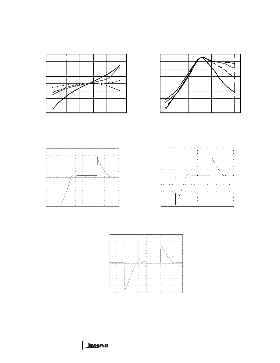
LOAD REGULATION
OUTPUT CURRENT (mA)
-20
-10
0
10
20
-0.2
-0.1
0
0.1
0.2
0.3
0.4
0.5
0.6
De
lta
V
OU
T
(mV)
-0.3
-15
-5
5
15
SOURCING
SINKING
-40°C
85°C
25°C
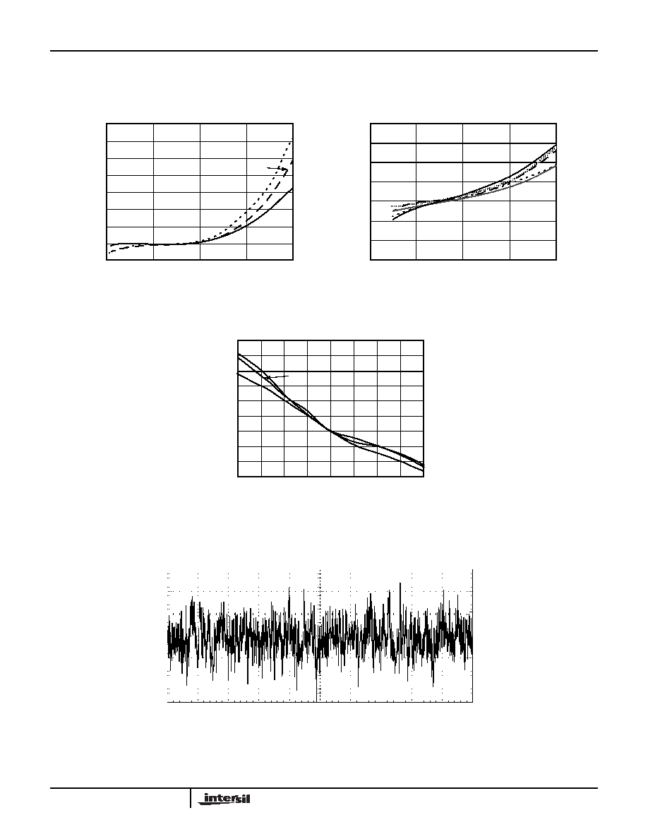
0.1Hz to 10Hz VOUT NOISE
10 Sec/div
5ĩ
V/d
i
v
Band Pass Filter with 1 zero at .1Hz and 2 poles at 10 Hz
X60008E-50
5
FN8145.0
March 14, 2005
TYPICAL PERFORMANCE CHARACTERISTIC CURVES
(V
IN
= 6.5V, I
OUT
= 0mA, T
A
= 25°C unless otherwise specified)
VOUT vs TEMPERATURE
TEMPERATURE (C)
-40C
-15C
10C
+35C
+60C
4.9980
4.9990
4.9995
5.0000
5.0005
5.0010
5.0015
5.0020
V
OU
T
(V)
4.9985
+85C
Normalized to 25°C
PSRR vs CAP LOAD
FREQUENCY (Hz)
1 Hz 10 Hz 100Hz 1kHz 10kHz
-80
-60
-50
-40
-30
-20
-10
0
PSRR (dB
)
-70
100kHz 1 MHz
4 Typical Units
C
L
=.001ĩF
C
L
=0
C
L
=.01ĩF
C
L
=.1ĩF
10mA LOAD TRANSIENT RESPONSE
10mA LOAD TRANSIENT RESPONSE
10mA LOAD TRANSIENT RESPONSE
2
00m
V/DIV
2
00m
V/DIV
2
00mV/DIV
C
L
= .001ĩF
I
IN
= -10mA
I
IN
= +10mA
500ĩSEC/DIV
500ĩSEC/DIV
500ĩSEC/DIV
C
L
= .1ĩF
I
IN
= -10mA
I
IN
= +10mA
C
L
= .01ĩF
I
IN
= -10mA
I
IN
= +10mA
X60008E-50