
1
®
FN9221.0
ISL6609, ISL6609A
Synchronous Rectified MOSFET Driver
The ISL6609, ISL6609A is a high frequency, MOSFET driver
optimized to drive two N-Channel power MOSFETs in a
synchronous-rectified buck converter topology. This driver
combined with an Intersil ISL63xx or ISL65xx multiphase
PWM controller forms a complete single-stage core-voltage
regulator solution with high efficiency performance at high
switching frequency for advanced microprocessors.
The IC is biased by a single low voltage supply (5V),
minimizing driver switching losses in high MOSFET gate
capacitance and high switching frequency applications.
Each driver is capable of driving a 3nF load with less than
10ns rise/fall time. Bootstrapping of the upper gate driver is
implemented via an internal low forward drop diode,
reducing implementation cost, complexity, and allowing the
use of higher performance, cost effective N-Channel
MOSFETs. Adaptive shoot-through protection is integrated
to prevent both MOSFETs from conducting simultaneously.
The ISL6609, ISL6609A features 4A typical sink current for
the lower gate driver, enhancing the lower MOSFET gate
hold-down capability during PHASE node rising edge,
preventing power loss caused by the self turn-on of the lower
MOSFET due to the high dV/dt of the switching node.
The ISL6609, ISL6609A also features an input that
recognizes a high-impedance state, working together with
Intersil multiphase PWM controllers to prevent negative
transients on the controlled output voltage when operation is
suspended. This feature eliminates the need for the schottky
diode that may be utilized in a power system to protect the
load from negative output voltage damage. In addition, the
ISL6609A's bootstrap function is designed to prevent the
BOOT capacitor from overcharging, should excessively large
negative swings occur at the transitions of the PHASE node.
Features
· Drives Two N-Channel MOSFETs
· Adaptive Shoot-Through Protection
· 0.4
On-Resistance and 4A Sink Current Capability
· Supports High Switching Frequency
- Fast Output Rise and Fall
- Ultra Low Three-State Hold-Off Time (20ns)
· ISL6605 Replacement with Enhanced Performance
· BOOT Capacitor Overcharge Prevention (ISL6609A)
· Low V
F
Internal Bootstrap Diode
· Low Bias Supply Current
· Enable Input and Power-On Reset
· QFN Package
- Compliant to JEDEC PUB95 MO-220 QFN-Quad Flat
No Leads-Product Outline
- Near Chip-Scale Package Footprint; Improves PCB
Efficiency and Thinner in Profile
· Pb-Free Plus Anneal Available (RoHS Compliant)
Applications
· Core Voltage Supplies for Intel® and AMD®
Microprocessors
· High Frequency Low Profile High Efficiency DC/DC
Converters
· High Current Low Voltage DC/DC Converters
· Synchronous Rectification for Isolated Power Supplies
Related Literature
· Technical Brief TB363 "Guidelines for Handling and
Processing Moisture Sensitive Surface Mount Devices
(SMDs)"
Ordering Information
PART NUMBER
(Note)
TEMP.
RANGE (°C)
PACKAGE
(Pb-Free)
PKG.
DWG. #
ISL6609CBZ
0 to 70
8 Ld SOIC
M8.15
ISL6609CRZ
0 to 70
8 Ld 3x3 QFN
L8.3x3
ISL6609ACBZ
0 to 70
8 Ld SOIC
M8.15
ISL6609ACRZ
0 to 70
8 Ld 3x3 QFN
L8.3x3
Add "-T" suffix for tape and reel.
NOTE: Intersil Pb-free plus anneal products employ special Pb-free
material sets; molding compounds/die attach materials and 100%
matte tin plate termination finish, which are RoHS compliant and
compatible with both SnPb and Pb-free soldering operations. Intersil
Pb-free products are MSL classified at Pb-free peak reflow
temperatures that meet or exceed the Pb-free requirements of
IPC/JEDEC J STD-020.
Data Sheet
August 10, 2005
CAUTION: These devices are sensitive to electrostatic discharge; follow proper IC Handling Procedures.
1-888-INTERSIL or 1-888-468-3774
|
Intersil (and design) is a registered trademark of Intersil Americas Inc.
Copyright Intersil Americas Inc. 2005. All Rights Reserved. Intel® is a registered trademark of Intel Corporation.
AMD® is a registered trademark of Advanced Micro Devices, Inc.
All other trademarks mentioned are the property of their respective owners.
2
FN9221.0
August 10, 2005
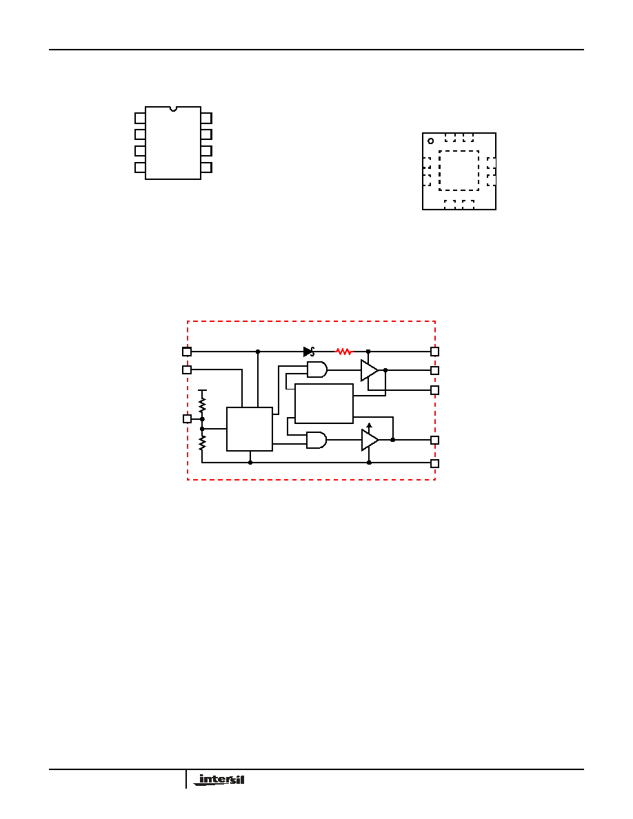
Pinouts
ISL6609/09A(SOIC)
TOP VIEW
ISL6609/09A (QFN)
TOP VIEW
Block Diagram
ISL6609 and ISL6609A
UGATE
BOOT
PWM
GND
1
2
3
4
8
7
6
5
PHASE
EN
VCC
LGATE
7
UGA
T
E
PHASE
8
4
3
1
2
6
GN
D
LG
A
T
E
EN
VCC
BOOT
PWM
5
6
VCC
PWM
VCC
4.25K
4K
CONTROL
LOGIC
SHOOT-
THROUGH
PROTECTION
BOOT
UGATE
PHASE
LGATE
GND
VCC
EN
R
BOOT
INTEGRATED 3
RESISTOR (R
BOOT
) AVAILABLE ONLY IN ISL6609A
ISL6609, ISL6609A

3
FN9221.0
August 10, 2005
Typical Application - Multiphase Converter Using ISL6609 Gate Drivers
+5V
BOOT
UGATE
PHASE
LGATE
PWM
EN
VCC
V
IN
+V
CORE
PGOOD
VID
FS/EN
GND
ISEN2
ISEN1
PWM2
PWM1
VSEN
PWM
FB
VCC
+5V
COMP
ISL6609
CONTROL
+5V
(ISL63XX
(OPTIONAL)
or ISL65XX)
R
UGPH
IS REQUIRED FOR SPECIAL POWER SEQUENCING APPLICATIONS
R
UGPH
(SEE APPLICATION INFORMATION SECTION ON PAGE 8)
+5V
BOOT
UGATE
PHASE
LGATE
PWM
EN
VCC
V
IN
ISL6609
R
UGPH
ISL6609, ISL6609A
4
FN9221.0
August 10, 2005
Absolute Maximum Ratings
Thermal Information
Supply Voltage (VCC) . . . . . . . . . . . . . . . . . . . . . . . . . . -0.3V to 7V
Input Voltage (V
EN
, V
PWM
) . . . . . . . . . . . . . . . -0.3V to VCC + 0.3V
BOOT Voltage (V
BOOT-GND
). . . -0.3V to 25V (DC) or 36V (<200ns)
BOOT To PHASE Voltage (V
BOOT-PHASE
) . . . . . . -0.3V to 7V (DC)
-0.3V to 9V (<10ns)
PHASE Voltage . . . . . . . . . . . . . . . . . . . . . GND - 0.3V to 15V (DC)
GND -8V (<20ns Pulse Width, 10
µJ) to 30V (<100ns)
UGATE Voltage . . . . . . . . . . . . . . . . V
PHASE
- 0.3V (DC) to V
BOOT
V
PHASE
- 5V (<20ns Pulse Width, 10
µJ) to V
BOOT
LGATE Voltage . . . . . . . . . . . . . . . GND - 0.3V (DC) to VCC + 0.3V
GND - 2.5V (<20ns Pulse Width, 5
µJ) to VCC + 0.3V
Ambient Temperature Range . . . . . . . . . . . . . . . . . . .-40°C to 125°C
HBM ESD Rating . . . . . . . . . . . . . . . . . . . . . . . . . . . . . . . . . . . . .2kV
Recommended Operating Conditions
Ambient Temperature Range . . . . . . . . . . . . . . . . . . .-40°C to 100°C
Maximum Operating Junction Temperature . . . . . . . . . . . . . . 125°C
Supply Voltage, VCC . . . . . . . . . . . . . . . . . . . . . . . . . . . . . 5V
±10%
Thermal Resistance (Notes 1, 2, & 3)
JA
(°C/W)
JC
(°C/W)
SOIC Package (Note 1) . . . . . . . . . . . .
110
N/A
QFN Package (Notes 2 & 3) . . . . . . . .
95
36
Maximum Junction Temperature . . . . . . . . . . . . . . . . . . . . . . . 150°C
Maximum Storage Temperature Range . . . . . . . . . . . -65°C to 150°C
Maximum Lead Temperature (Soldering 10s) . . . . . . . . . . . . . 300°C
(SOIC - Lead Tips Only)
CAUTION: Stresses above those listed in "Absolute Maximum Ratings" may cause permanent damage to the device. This is a stress only rating and operation of the
device at these or any other conditions above those indicated in the operational sections of this specification is not implied.
NOTES:
1.
JA
is measured with the component mounted on a high effective thermal conductivity test board in free air. See Tech Brief TB379 for details.
2.
JA
is measured in free air with the component mounted on a high effective thermal conductivity test board with "direct attach" features.
3.
JC
, "case temperature" location is at the center of the package underside exposed pad. See Tech Brief TB379 for details.
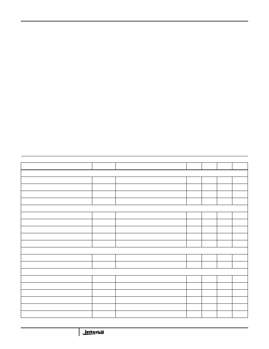
Electrical Specifications
These specifications apply for T
A
= -40°C to 100°C, unless otherwise noted
PARAMETER
SYMBOL
TEST CONDITIONS
MIN
TYP
MAX
UNITS
VCC SUPPLY CURRENT
Bias Supply Current
I
VCC
PWM pin floating, V
VCC
= 5V
-
132
-
µA
POR Rising
-
3.4
4.2
POR Falling
2.2
3.0
-
Hysteresis
-
400
-
mV
PWM INPUT
Sinking Impedance
R
PWM_SNK
2.75
4
5.5
k
Source Impedance
R
PWM_SRC
3
4.25
5.75
k
Three-State Rising Threshold
V
VCC
= 5V (100mV Hysteresis)
-
1.70
2.00
V
Three-State Falling Threshold
V
VCC
= 5V (100mV Hysteresis)
3.10
3.41
-
V
Three-State Shutdown Holdoff Time
t
TSSHD
t
PDLU
or t
PDLL
+ Gate Falling Time
-
20
-
ns
EN INPUT
EN LOW Threshold
1.0
1.3
-
V
EN HIGH Threshold
-
1.6
2.0
V
SWITCHING TIME (See Figure 1 on Page 6)
UGATE Rise Time (Note 4)
t
RU
V
VCC
= 5V, 3nF Load
-
8.0
-
ns
LGATE Rise Time (Note 4)
t
RL
V
VCC
= 5V, 3nF Load
-
8.0
-
ns
UGATE Fall Time (Note 4)
t
FU
V
VCC
= 5V, 3nF Load
-
8.0
-
ns
LGATE Fall Time (Note 4)
t
FL
V
VCC
= 5V, 3nF Load
-
4.0
-
ns
UGATE Turn-Off Propagation Delay
t
PDLU
V
VCC
= 5V, Outputs Unloaded
-
18
-
ns
LGATE Turn-Off Propagation Delay
t
PDLL
V
VCC
= 5V, Outputs Unloaded
-
25
-
ns
ISL6609, ISL6609A
5
FN9221.0
August 10, 2005
Functional Pin Description
Note: Pin numbers refer to the SOIC package. Check
diagram for corresponding QFN pinout.
UGATE (Pin 1)
Upper gate drive output. Connect to gate of high-side
N-Channel power MOSFET. A gate resistor is never
recommended on this pin, as it interferes with the operation
shoot-through protection circuitry.
BOOT (Pin 2)
Floating bootstrap supply pin for the upper gate drive.
Connect a bootstrap capacitor between this pin and the
PHASE pin. The bootstrap capacitor provides the charge
used to turn on the upper MOSFET. See the Bootstrap
Considerations section for guidance in choosing the
appropriate capacitor value.
PWM (Pin 3)
The PWM signal is the control input for the driver. The PWM
signal can enter three distinct states during operation, see the
Three-state PWM Input section for further details. Connect this
pin to the PWM output of the controller.
GND (Pin 4)
Ground pin. All signals are referenced to this node.
LGATE (Pin 5)
Lower gate drive output. Connect to gate of the low side
N-Channel power MOSFET. A gate resistor is never
recommended on this pin, as it interferes with the operation
shoot-through protection circuitry.
VCC (Pin 6)
Connect this pin to a +5V bias supply. Locally bypass with a
high quality ceramic capacitor to ground.
EN (Pin 7)
Enable input pin. Connect this pin high to enable and low to
disable the driver.
PHASE (Pin 8)
Connect this pin to the source of the upper MOSFET. This
pin provides the return path for the upper gate driver current.
Thermal Pad (in QFN only)
The metal pad underneath the center of the IC is a thermal
substrate. The PCB "thermal land" design for this exposed
die pad should include vias that drop down and connect to
one or more buried copper plane(s). This combination of
vias for vertical heat escape and buried planes for heat
spreading allows the QFN to achieve its full thermal
potential. This pad should be either grounded or floating,
and it should not be connected to other nodes. Refer to
TB389 for design guidelines.
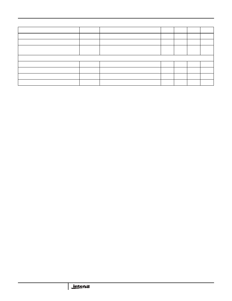
UGATE Turn-On Propagation Delay
t
PDHU
V
VCC
= 5V, Outputs Unloaded
-
18
-
ns
LGATE Turn-On Propagation Delay
t
PDHL
V
VCC
= 5V, Outputs Unloaded
-
23
-
ns
Three-state to UG/LG Rising Propagation
Delay
t
PTS
V
VCC
= 5V, Outputs Unloaded
-
20
-
ns
OUTPUT
Upper Drive Source Resistance
R
UG_SRC
250mA Source Current
-
1.0
2.5
Upper Drive Sink Resistance
R
UG_SNK
250mA Sink Current
-
1.0
2.5
Lower Drive Source Resistance
R
LG_SRC
250mA Source Current
-
1.0
2.5
Lower Drive Sink Resistance
R
LG_SNK
250mA Sink Current
-
0.4
1.0
NOTE:
4. Guaranteed by Characterization. Not 100% tested in production.
Electrical Specifications
These specifications apply for T
A
= -40°C to 100°C, unless otherwise noted (Continued)
PARAMETER
SYMBOL
TEST CONDITIONS
MIN
TYP
MAX
UNITS
ISL6609, ISL6609A