2-152
HIP6012
Buck and Synchronous-Rectifier
Pulse-Width Modulator (PWM) Controller
The HIP6012 provides complete control and protection for a
DC-DC converter optimized for high-performance
microprocessor applications. It is designed to drive two
N-Channel MOSFETs in a synchronous-rectified buck
topology. The HIP6012 integrates all of the control, output
adjustment, monitoring and protection functions into a single
package.
The output voltage of the converter can be precisely
regulated to as low as 1.27V, with a maximum tolerance of
±
1.5% over temperature and line voltage variations.
The HIP60012 provides simple, single feedback loop,
voltage-mode control with fast transient response. It includes
a 200kHz free-running triangle-wave oscillator that is
adjustable from below 50kHz to over 1MHz. The error
amplifier features a 15MHz gain-bandwidth product and
6V/
µ
s slew rate which enables high converter bandwidth for
fast transient performance. The resulting PWM duty ratio
ranges from 0% to 100%.
The HIP6012 protects against over-current conditions by
inhibiting PWM operation. The HIP6012 monitors the current
by using the r
DS(ON)
of the upper MOSFET which eliminates
the need for a current sensing resistor.
Pinout
HIP6012
(SOIC)
TOP VIEW
Features
· Drives Two N-Channel MOSFETs
· Operates From +5V or +12V Input
· Simple Single-Loop Control Design
- Voltage-Mode PWM Control
· Fast Transient Response
- High-Bandwidth Error Amplifier
- Full 0% to 100% Duty Ratio
· Excellent Output Voltage Regulation
- 1.27V Internal Reference
-
±
1.5% Over Line Voltage and Temperature
· Over-Current Fault Monitor
- Does Not Require Extra Current Sensing Element
- Uses MOSFETs r
DS(ON)
· Small Converter Size
- Constant Frequency Operation
- 200kHz Free-Running Oscillator Programmable from
50kHz to Over 1MHz
· 14 Pin, SOIC Package
Applications
· Power Supply for Pentium®, Pentium Pro, PowerPCTM and
AlphaTM Microprocessors
· High-Power 5V to 3.xV DC-DC Regulators
· Low-Voltage Distributed Power Supplies
PowerPCTM is a trademark of IBM.
AlphaTM is a trademark of Digital Equipment Corporation.
Pentium® is a registered trademark of Intel Corporation.
8
9
10
11
12
13
14
7
6
5
4
3
2
1
OCSET
SS
EN
COMP
FB
RT
VCC
LGATE
PGND
BOOT
UGATE
PHASE
GND
PVCC
Ordering Information
PART NUMBER
TEMP.
RANGE (
o
C)
PACKAGE
PKG.
NO.
HIP6012CB
0 to 70
14 Ld SOIC
M14.15
Data Sheet
June 1997
File Number
4324
CAUTION: These devices are sensitive to electrostatic discharge; follow proper IC Handling Procedures.
http://www.intersil.com or 407-727-9207
|
Copyright
©
Intersil Corporation 1999
2-153
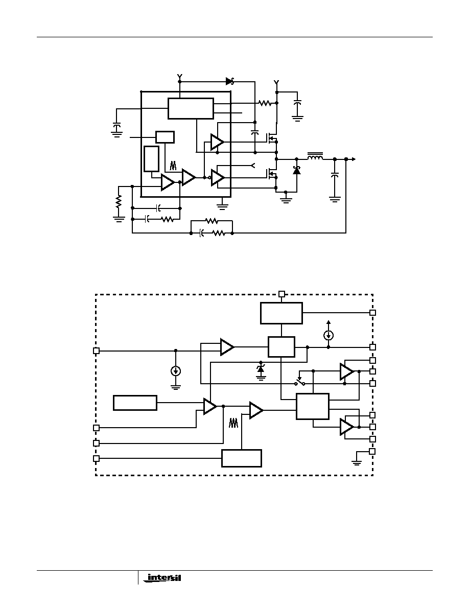
Typical Application
Block Diagram
12V
+V
O
PGND
HIP6012
RT
FB
COMP
SS
GND
OSC
LGATE
UGATE
OCSET
PHASE
BOOT
EN
VCC
+5V OR +12V
PVCC
+12V
MONITOR AND
PROTECTION
REF
+
-
+
-
OSCILLATOR
SOFT-
START
POWER-ON
RESET (POR)
INHIBIT
PWM
COMPARATOR
ERROR
AMP
VCC
SS
PWM
RT
GND
OCSET
FB
COMP
EN
1.27 VREF
OVER-
CURRENT
GATE
CONTROL
LOGIC
BOOT
UGATE
LGATE
PHASE
PGND
200
µ
A
PVCC
10
µ
A
4V
REFERENCE
+
-
+
-
+
-
HIP6012

2-154
Absolute Maximum Ratings
Thermal Information
Supply Voltage, V
CC
. . . . . . . . . . . . . . . . . . . . . . . . . . . . . . . +15.0V
Boot Voltage, V
BOOT
- V
PHASE
. . . . . . . . . . . . . . . . . . . . . . . +15.0V
Input, Output or I/O Voltage . . . . . . . . . . . . GND -0.3V to V
CC
+0.3V
ESD Classification . . . . . . . . . . . . . . . . . . . . . . . . . . . . . . . . . Class 2
Operating Conditions
Supply Voltage, V
CC
. . . . . . . . . . . . . . . . . . . . . . . . . . . +12V
±
10%
Ambient Temperature Range . . . . . . . . . . . . . . . . . . . . . 0
o
C to 70
o
C
Junction Temperature Range . . . . . . . . . . . . . . . . . . . . 0
o
C to 125
o
C
Thermal Resistance (Typical, Note 1)
JA
(
o
C/W)
SOIC Package . . . . . . . . . . . . . . . . . . . . . . . . . . . . .
115
Maximum Junction Temperature . . . . . . . . . . . . . . . . . . . . . . 150
o
C
Maximum Storage Temperature Range . . . . . . . . . . -65
o
C to 150
o
C
Maximum Lead Temperature (Soldering 10s) . . . . . . . . . . . . 300
o
C
(Lead tips only)
CAUTION: Stresses above those listed in "Absolute Maximum Ratings" may cause permanent damage to the device. This is a stress only rating and operation of the
device at these or any other conditions above those indicated in the operational sections of this specification is not implied.
NOTE:
1.
JA
is measured with the component mounted on an evaluation PC board in free air.
Electrical Specifications
Recommended Operating Conditions, Unless Otherwise Noted
PARAMETER
SYMBOL
TEST CONDITIONS
MIN
TYP
MAX
UNITS
VCC SUPPLY CURRENT
Nominal Supply
I
CC
EN = V
CC
; UGATE and LGATE Open
-
5
-
mA
Shutdown Supply
EN = 0V
-
50
100
µ
A
POWER-ON RESET
Rising V
CC
Threshold
V
OCSET
= 4.5VDC
-
-
10.4
V
Falling V
CC
Threshold
V
OCSET
= 4.5VDC
8.8
-
-
V
Enable - Input threshold Voltage
V
OCSET
= 4.5VDC
0.8
-
2.0
V
Rising V
OCSET
Threshold
-
1.27
-
V
OSCILLATOR
Free Running Frequency
R
T
= OPEN, V
CC
= 12
180
200
220
kHz
Total Variation
6k
< R
T
to GND < 200k
-20
-
+20
%
Ramp Amplitude
V
OSC
R
T
= OPEN
-
1.9
-
V
P-P
REFERENCE
Reference Voltage
1.251
1.270
1.289
V
ERROR AMPLIFIER
DC Gain
-
88
-
dB
Gain-Bandwidth Product
GBW
-
15
-
MHz
Slew Rate
SR
COMP = 10pF
-
6
-
V/
µ
s
GATE DRIVERS
Upper Gate Source
I
UGATE
V
BOOT
- V
PHASE
= 12V, V
UGATE
= 6V
350
500
-
mA
Upper Gate Sink
R
UGATE
I
LGATE
= 0.3A
-
5.5
10
Lower Gate Source
I
LGATE
V
CC
= 12V, V
LGATE
= 6V
300
450
-
mA
Lower Gate Sink
R
LGATE
I
LGATE
= 0.3A
-
3.5
6.5
PROTECTION
OCSET Current Source
I
OCSET
V
OCSET
= 4.5VDC
170
200
230
µ
A
Soft Start Current
I
SS
-
10
-
µ
A
HIP6012
2-155
Functional Pin Description
RT (Pin 1)
This pin provides oscillator switching frequency adjustment.
By placing a resistor (R
T
) from this pin to GND, the nominal
200kHz switching frequency is increased according to the
following equation:
Conversely, connecting a pull-up resistor (R
T
) from this pin
to V
CC
reduces the switching frequency according to the
following equation.:
OCSET (Pin 2)
Connect a resistor (R
OCSET
) from this pin to the drain of the
upper MOSFET. R
OCSET
, an internal 200
µ
A current source
(I
OCS
), and the upper MOSFET on-resistance (r
DS(ON)
) set
the converter over-current (OC) trip point according to the
following equation:
An over-current trip cycles the soft-start function.
SS (Pin 3)
Connect a capacitor from this pin to ground. This capacitor,
along with an internal 10
µ
A current source, sets the soft-
start interval of the converter.
COMP (Pin 4) and FB (Pin 5)
COMP and FB are the available external pins of the error
amplifier. The FB pin is the inverting input of the error
amplifier and the COMP pin is the error amplifier output.
These pins are used to compensate the voltage-control
feedback loop of the converter.
EN (Pin 6)
This pin is the open-collector enable pin. Pull this pin below
1V to disable the converter. In shutdown, the soft start pin is
discharged and the UGATE and LGATE pins are held low.
GND (Pin 7)
Signal ground for the IC. All voltage levels are measured with
respect to this pin.
PHASE (Pin 8)
Connect the PHASE pin to the upper MOSFET source. This
pin is used to monitor the voltage drop across the MOSFET
for over-current protection. This pin also provides the return
path for the upper gate drive.
UGATE (Pin 9)
Connect UGATE to the upper MOSFET gate. This pin
provides the gate drive for the upper MOSFET.
BOOT (Pin 10)
This pin provides bias voltage to the upper MOSFET driver.
A bootstrap circuit may be used to create a BOOT voltage
suitable to drive a standard N-Channel MOSFET.
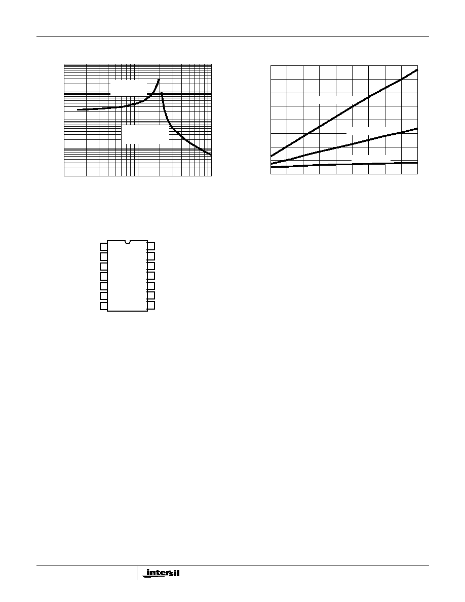
Typical Performance Curves
FIGURE 1. R
T
RESISTANCE vs FREQUENCY
FIGURE 2. BIAS SUPPLY CURRENT vs FREQUENCY
10
100
1000
SWITCHING FREQUENCY (kHz)
RESIST
ANCE (k
)
10
100
1000
R
T
PULLUP
TO +12V
R
T
PULLDOWN
TO V
SS
100
200
300
400
500
600
700
800
900
1000
80
70
60
50
40
30
20
10
0
I
VCC
(mA)
SWITCHING FREQUENCY (kHz)
C
GATE
= 1000pF
C
GATE
= 3300pF
C
GATE
= 10pF
8
9
10
11
12
13
14
7
6
5
4
3
2
1
OCSET
SS
EN
COMP
FB
RT
VCC
LGATE
PGND
BOOT
UGATE
PHASE
GND
PVCC
Fs
200kHz
5
10
6
·
R
T
------------------
+
(R
T
to GND)
Fs
200kHz
4
10
7
·
R
T
------------------
(R
T
to 12V)
I
PEAK
I
OCS
R
OCSET
·
r
DS ON
(
)
--------------------------------------------
=
HIP6012
2-156
PGND (Pin 11)
This is the power ground connection. Tie the lower MOSFET
source to this pin.
LGATE (Pin 12)
Connect LGATE to the lower MOSFET gate. This pin
provides the gate drive for the lower MOSFET.
PVCC (Pin 13)
Provide a bias supply for the lower gate drive to this pin.
VCC (Pin 14)
Provide a 12V bias supply for the chip to this pin.
Functional Description
Initialization
The HIP6012 automatically initializes upon receipt of power.
Special sequencing of the input supplies is not necessary.
The Power-On Reset (POR) function continually monitors
the input supply voltages and the enable (EN) pin. The POR
monitors the bias voltage at the VCC pin and the input
voltage (V
IN
) on the OCSET pin. The level on OCSET is
equal to V
IN
Less a fixed voltage drop (see over-current
protection). With the EN pin held to V
CC
, the POR function
initiates soft start operation after both input supply voltages
exceed their POR thresholds. For operation with a single
+12V power source, V
IN
and V
CC
are equivalent and the
+12V power source must exceed the rising V
CC
threshold
before POR initiates operation.
The Power-On Reset (POR) function inhibits operation with
the chip disabled (EN pin low). With both input supplies
above their POR thresholds, transitioning the EN pin high
initiates a soft start interval.
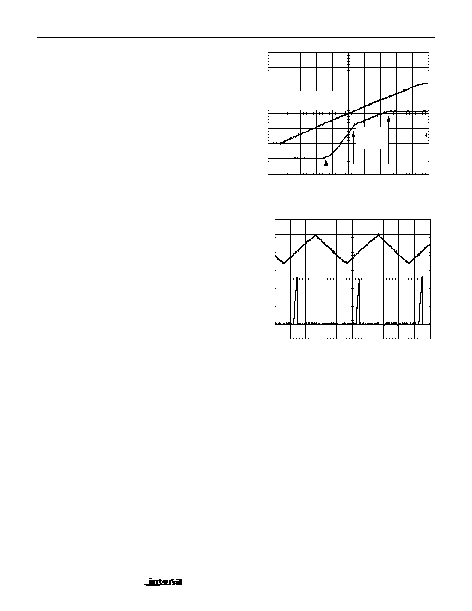
Soft Start
The POR function initiates the soft start sequence. An internal
10
µ
A current source charges an external capacitor (C
SS
) on
the SS pin to 4V. Soft start clamps the error amplifier output
(COMP pin) and reference input (+ terminal of error amp) to
the SS pin voltage. Figure 3 shows the soft start interval with
C
SS
= 0.1
µ
F. Initially the clamp on the error amplifier (COMP
pin) controls the converter's output voltage. At t1 in Figure 3,
the SS voltage reaches the valley of the oscillator's triangle
wave. The oscillator's triangular waveform is compared to the
ramping error amplifier voltage. This generates PHASE
pulses of increasing width that charge the output capacitor(s).
This interval of increasing pulse width continues to t2. With
sufficient output voltage, the clamp on the reference input
controls the output voltage. This is the interval between t2 and
t3 in Figure 3. At t3 the SS voltage exceeds the reference
voltage and the output voltage is in regulation. This method
provides a rapid and controlled output voltage rise.
Over-Current Protection
The over-current function protects the converter from a
shorted output by using the upper MOSFETs on-resistance,
r
DS(ON)
to monitor the current. This method enhances the
converter's efficiency and reduces cost by eliminating a
current sensing resistor.
The over-current function cycles the soft-start function in a
hiccup mode to provide fault protection. A resistor (R
OCSET
)
programs the over-current trip level. An internal 200
µ
A
(typical) current sink develops a voltage across R
OCSET
that
is reference to V
IN
. When the voltage across the upper
MOSFET (also referenced to V
IN
) exceeds the voltage
across R
OCSET
, the over-current function initiates a soft-
start sequence. The soft-start function discharges C
SS
with
a 10
µ
A current sink and inhibits PWM operation. The soft-
start function recharges C
SS
, and PWM operation resumes
with the error amplifier clamped to the SS voltage. Should an
overload occur while recharging C
SS
, the soft start function
inhibits PWM operation while fully charging C
SS
to 4V to
complete its cycle. Figure 4 shows this operation with an
TIME (5ms/DIV)
SOFT-START
(1V/DIV)
0V
0V
t1
t2
t3
OUTPUT
(1V/DIV)
VOLTAGE
FIGURE 3. SOFT-START INTERVAL
OUTPUT INDUCT
OR
SOFT
-ST
AR
T
0A
0V
TIME (20ms/DIV)
5A
10A
15A
2V
4V
FIGURE 4. OVER-CURRENT OPERATION
HIP6012