2-8
File Number
4142
HIP5015, HIP5016
7V, 7A SynchroFETTM Complementary
Drive Synchronous Half-Bridge
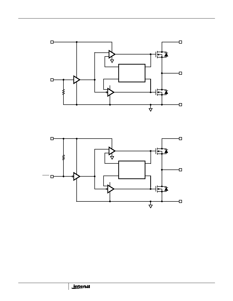
Designed with the Pentium® in mind, the Intersil SynchroFET
family provides a new approach for implementing a
synchronous rectified buck switching regulator. The
SynchroFETTM replaces two power DMOSs, a Schottky diode,
two gate drivers and synchronous control circuitry. The
complementary drive circuit turns the upper FET on and the
lower FET off when the input from the PWM is high. When the
input from the PWM goes low the upper FET turns off and the
lower FET turns on. The HIP5016 has a PWM pin that inverts
the relationship from the input to PHASE. This architecture
allows the designer to utilize a low cost single-ended PWM
controller in either a current or voltage mode configuration. The
SynchroFET operates in continuous conduction mode reducing
EMI constraints and enabling high bandwidth operation.
Several features ensure easy start-up. First, the supply currents
stay below specification as the supply voltages ramp up; no
unexpected surges occur that might perturb a soft-start or
deplete a charge-pump. Second, any power-up sequence of
the V
CC
, V
IN
, or PWM pins can be used without causing large
currents. Third, the chip operates when V
CC
is greater than 2V
so V
CC
can be created from a charge pump powered from V
IN
.
Features
· Complementary Drive, Half-Bridge Power NMOS
· Use With Low-Cost Single-Output PWM Controllers
· Improve Efficiency Over Conventional Buck Converter with
Schottky Clamp
· Minimum Deadtime Provided by Adaptive Shoot-Through
Protection Eliminates External Schottky
· Grounded Case for Low EMI and Simple Heatsinking
· Low Operating Current
· Frequency Exceeding 1MHz
· Dual Polarity Input Options
· All Pins Surge Protected
Applications
· 5V to
3.3V Synchronous Buck Converters
· 3.3V to
2.9V Synchronous Buck Converters
· Pentium Power Supplies
· Bus Terminations (BTL and GTL)
· Drive 5V Motors Directly from Microprocessor
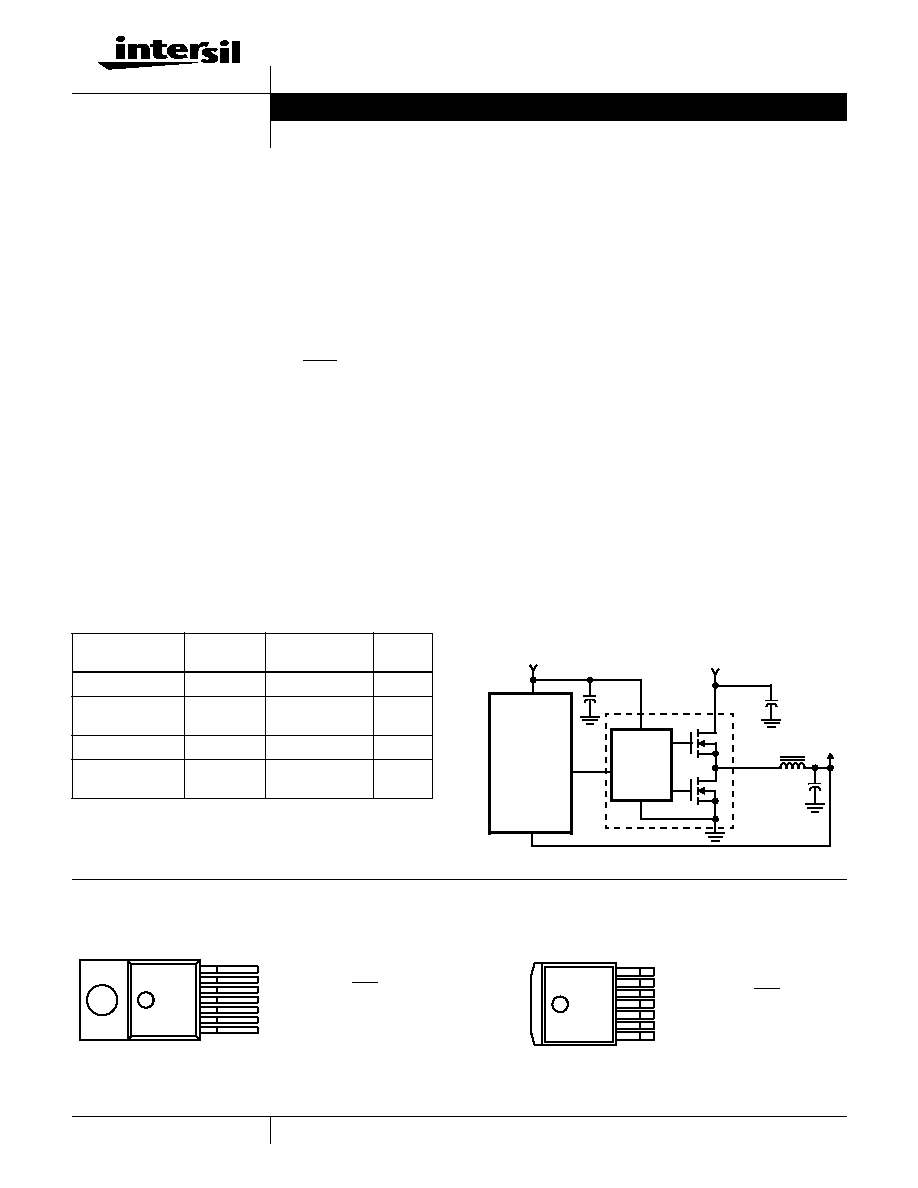
Typical Application Block Diagram
Pinouts
HIP5015IS1, HIP5016IS1 (SIP - VERTICAL)
TOP VIEW
Pentium® is a registered trademark of Intel Corporation.
SynchroFETTM is a trademark of Intersil Corporation.
HIP5015IS, HIP5016IS (SIP - GULLWING)
TOP VIEW
Ordering Information
PART NUMBER
TEMP.
RANGE (
o
C)
PACKAGE
PKG.
NO.
HIP5015IS
-40 to 85
7 Ld Gullwing SIP
Z7.05B
HIP5015IS1
-40 to 85
7 Ld Staggered
Vertical SIP
Z7.05C
HIP5016IS
-40 to 85
7 Ld Gullwing SIP
Z7.05B
HIP5016IS1
-40 to 85
7 Ld Staggered
Vertical SIP
Z7.05C
+12V
+3.3V
PHASE
PWM
V
IN
V
CC
CONTROL
+5V
HIP5015
PWM
CONTROLLER
SYNCHRONOUS RECTIFIED BUCK CONVERTER
GND
1 PHASE
2 V
IN
3 V
CC
4 GND
5 PWM (HIP5015), PWM (HIP5016)
6 NC
7 NC
GND (TAB)
FRONT ROWS = PINS 1,3,5,7
BACK ROWS = PINS 2,4,6
1 PHASE
2 V
IN
3 V
CC
4
5 PWM (HIP5015), PWM (HIP5016)
6 NC
7 NC
GND
(TAB)
Data Sheet
June 1996
CAUTION: These devices are sensitive to electrostatic discharge; follow proper IC Handling Procedures.
http://www.intersil.com or 407-727-9207
|
Copyright
©
Intersil Corporation 1999
2-10
Absolute Maximum Ratings
Thermal Information
(Typical)
Supply Voltage, V
CC
. . . . . . . . . . . . . . . . . . . . . . . . . . . . . . . . +16V
Input Voltage
V
IN
. . . . . . . . . . . . . . . . . . . . . . . . . . . . . . . . . . . . +7V
I
PHASE,
I
VIN,
I
GND
. . . . . . . . . . . . . . . . . . . . . 7A (Repetitive Peak)
PWM Input . . . . . . . . . . . . . . . . . . . . . . . . . . . . . . . . . . . -4V to +16V
ESD Classification . . . . . . . . . . . . . . . . . . . . . . . . . . . . Class 3 (4kV)
Lead Temperature (Soldering 10s) (Lead Tips Only). . . . . . . 300
o
C
Storage Temperature Range . . . . . . . . . . . . . . . . . . -65
o
C to 150
o
C
Junction Temperature Range . . . . . . . . . . . . . . . . . . -40
o
C to 150
o
C
Operating Conditions
Supply Voltage, V
CC
. . . . . . . . . . . . . . . . . . . . . . . . . . . +12V,
±
20%
Input Voltage
V
IN
. . . . . . . . . . . . . . . . . . . . . . . . . . . . . . . 0V to 5.5V
Supply Voltage, V
CC,
minimum for charge-pumped start-up . . . .+4.0V
Package
JC
JA
(
o
C/W)
(
o
C/W)
0
1
2
3
3
SIP (IS). . . . .
2
55
30
25
24
18
SIP (IS1). . . .
2
55
-
-
-
-
Versus additional square inches of 1 ounce copper on the
printed circuit board
.
JC
is typical with an infinite heatsink.
200 linear feet per minute of air flow.
I
PHASE
. . . . . . . . . . . . . . . . . . . . . . . . . . . . . . . . . . . . . . . . . . . . .5A
I
VIN
. . . . . . . . . . . . . . . . . . . . . . . . . . . . . . . . . . . . . . . . . . . . . . . .4A
I
GND
. . . . . . . . . . . . . . . . . . . . . . . . . . . . . . . . . . . . . . . . . . . . . . .3A
CAUTION: Stresses above those listed in "Absolute Maximum Ratings" may cause permanent damage to the device. This is a stress only rating and operation of the
device at these or any other conditions above those indicated in the recommended operating conditions of this specification is not implied.
Electrical Specifications
PARAMETER
SYMBOL
TEST CONDITIONS
T
J
= 25
o
C
T
J
= - 40
o
C
T
J
= +150
o
C
UNITS
MIN
TYP
MAX
MIN
MAX
r
DS(ON)
Upper MOSFET
R
DSU
V
CC
= 12V,
V
IN = 5V
-
68
78
-
130
m
r
DS(ON)
Lower MOSFET
R
DSL
V
CC
= 12V,
V
IN = 5V
-
72
82
-
136
m
V
IN
Operating Current
I
VINO
V
IN
= 5V, No Load, 500kHz
-
1.8
4
-
5
mA
V
IN
Quiescent Current
I
VIN
PWM or PWM =
V
CC
or GND
-
0.1
10
-
100
µ
A
V
CC
Operating Current
I
CCO
V
CC
= 12V, 500kHz
-
4.3
7
-
9
mA
V
CC
Quiescent Current (HIP5015)
I
CCIH
PWM =
V
CC
-
40
-
-
300
µ
A
V
CC
Quiescent Current (HIP5015)
I
CCIL
PWM = GND
-
0.1
10
-
100
µ
A
V
CC
Quiescent Current (HIP5016)
I
CCNIH
PWM =
V
CC
-
0.1
10
-
100
µ
A
V
CC
Quiescent Current (HIP5016)
I
CCNIL
PWM = GND
-
100
-
-
300
µ
A
Low Level PWM Input Voltage
V
IL
-
1.8
-
1
-
V
High Level PWM Input Voltage
V
IH
-
2.1
-
-
3
V
PWM Input Voltage Hysteresis
V
IHYS
-
0.3
-
-
-
V
Input Pulldown Resistance (HIP5015)
R
PWM
-
220
-
100
400
k
Input Pullup Resistance (HIP5016)
R
PWM
-
220
-
100
400
k
Switching Specifications
PARAMETER
SYMBOL
TEST CONDITIONS
T
J
= 25
o
C
T
J
= - 40
o
C
T
J
= +150
o
C
UNITS
MIN
TYP
MAX
MIN
MAX
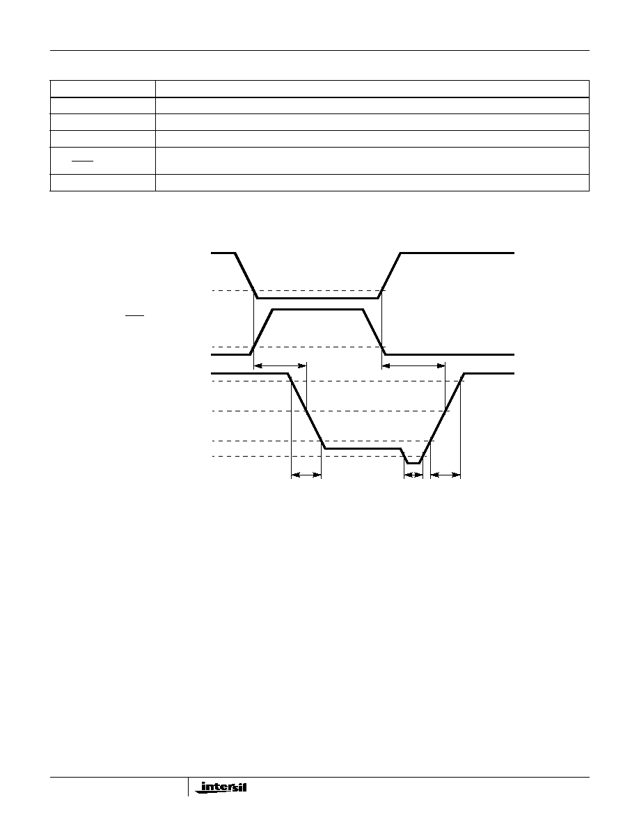
Upper Device Turn-Off Delay
t
PHL
V
CC
= 12V, I
PHASE
= -0.5A
-
30
50
-
80
ns
Lower Device Turn-Off Delay
t
PLH
V
CC
= 12V, I
PHASE
= +0.5A
-
30
50
-
80
ns
Dead Time
t
DT
V
CC
= +12V, I
PHASE
= -0.5A
-
10
-
-
-
ns
Phase Rise-Time
t
r
V
CC
= 12V, I
PHASE
= -0.5A
-
20
-
-
-
ns
Phase Fall-Time
t
f
V
CC
= 12V, I
PHASE
= +0.5A
-
20
-
-
-
ns
HIP5015, HIP5016