1
HIP4081A
80V/2.5A Peak, High Frequency
Full Bridge FET Driver
Description
The HIP4081A is a high frequency, medium voltage Full
Bridge N-Channel FET driver IC, available in 20 lead plastic
SOIC and DIP packages. The HIP4081A can drive every
possible switch combination except those which would
cause a shoot-through condition. The HIP4081A can switch
at frequencies up to 1MHz and is well suited to driving Voice
Coil Motors, high-frequency Class D audio amplifiers, and
power supplies.
For example, the HIP4081A can drive medium voltage brush
motors, and two HIP4081As can be used to drive high per-
formance stepper motors, since the short minimum "on-time"
can provide fine micro-stepping capability.
Short propagation delays of approximately 55ns maximizes
control loop crossover frequencies and dead-times which
can be adjusted to near zero to minimize distortion, resulting
in rapid, precise control of the driven load.
A similar part, the HIP4080A, includes an on-chip input com-
parator to create a PWM signal from an external triangle
wave and to facilitate "hysteresis mode" switching.
The Application Note for the HIP4081A is the AN9405.
Ordering Information
PART
NUMBER
TEMP RANGE
(
o
C)
PACKAGE
PKG. NO.
HIP4081AIP
-40 to 85
20 Ld PDIP
E20.3
HIP4081AIB
-40 to 85
20 Ld SOIC (W)
M20.3
Features
· Independently Drives 4 N-Channel FET in Half Bridge
or Full Bridge Configurations
· Bootstrap Supply Max Voltage to 95V
DC
· Drives 1000pF Load at 1MHz in Free Air at 50
o
C with
Rise and Fall Times of Typically 10ns
· User-Programmable Dead Time
· On-Chip Charge-Pump and Bootstrap Upper Bias
Supplies
· DIS (Disable) Overrides Input Control
· Input Logic Thresholds Compatible with 5V to 15V
Logic Levels
· Very Low Power Consumption
· Undervoltage Protection
Applications
· Medium/Large Voice Coil Motors
· Full Bridge Power Supplies
· Class D Audio Power Amplifiers
· High Performance Motor Controls
· Noise Cancellation Systems
· Battery Powered Vehicles
· Peripherals
· U.P.S.
November 1996
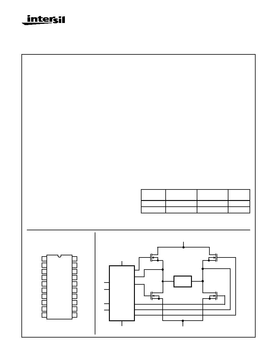
Pinout
HIP4081A (PDIP, SOIC)
TOP VIEW
11
12
13
14
15
16
17
18
20
19
10
9
8
7
6
5
4
3
2
1
BHB
BHI
DIS
V
SS
BLI
ALI
HDEL
AHI
LDEL
AHB
BHO
BLO
BLS
V
DD
BHS
V
CC
ALS
ALO
AHS
AHO
Application Block Diagram
80V
GND
LOAD
HIP4081A
GND
12V
AHI
ALI
BLI
BHI
BLO
BHS
BHO
ALO
AHS
AHO
File Number
3659.5
CAUTION: These devices are sensitive to electrostatic discharge; follow proper IC Handling Procedures.
www.intersil.com or 407-727-9207
|
Copyright
©
Intersil Corporation 1999

2
HIP4081A
Functional Block Diagram
(1/2 HIP4081A)
Typical Application
(PWM Mode Switching)
CHARGE
PUMP
V
DD
AHI
DIS
ALI
HDEL
LDEL
V
SS
TURN-ON
DELAY
TURN-ON
DELAY
DRIVER
DRIVER
AHB
AHO
AHS
V
CC
ALO
ALS
C
BF
TO V
DD
(PIN 16)
C
BS
D
BS
HIGH VOLTAGE BUS
80V
DC
+12V
DC
LEVEL SHIFT
AND LATCH
14
10
11
12
15
13
16
7
3
6
8
9
4
BIAS
SUPPLY
UNDER-
VOLTAGE
11
12
13
14
15
16
17
18
20
19
10
9
8
7
6
5
4
3
2
1 BHB
BHI
DIS
V
SS
BLI
ALI
HDEL
AHI
LDEL
AHB
BHO
BLO
BLS
V
DD
BHS
V
CC
ALS
ALO
AHS
AHO
80V
12V
+
-
12V
DIS
GND
6V
GND
TO OPTIONAL
CURRENT CONTROLLER
PWM
LOAD
INPUT
HIP4081/HIP4081A
3
HIP4081A
Absolute Maximum Ratings
Thermal Information
Supply Voltage, V
DD
and V
CC
. . . . . . . . . . . . . . . . . . . . -0.3V to 16V
Logic I/O Voltages . . . . . . . . . . . . . . . . . . . . . . . -0.3V to V
DD
+0.3V
Voltage on AHS, BHS . . . . -6.0V (Transient) to 80V (25
o
C to 125
o
C)
Voltage on AHS, BHS . . . -6.0V (Transient) to 70V (-55
o
C to 125
o
C)
Voltage on ALS, BLS . . . . . . . -2.0V (Transient) to +2.0V (Transient)
Voltage on AHB, BHB . . . . . . . . . V
AHS, BHS
-0.3V to V
AHS, BHS
+V
DD
Voltage on ALO, BLO . . . . . . . . . . . . . V
ALS, BLS
-0.3V to V
CC
+0.3V
Voltage on AHO, BHO . . . . . . . V
AHS, BHS
-0.3V to V
AHB, BHB
+0.3V
Input Current, HDEL and LDEL . . . . . . . . . . . . . . . . . . -5mA to 0mA
Phase Slew Rate . . . . . . . . . . . . . . . . . . . . . . . . . . . . . . . . . . 20V/ns
NOTE: All Voltages relative to V
SS
, unless otherwise specified.
Thermal Resistance (Typical, Note 1)
JA
(
o
C/W)
SOIC Package . . . . . . . . . . . . . . . . . . . . . . . . . . . . .
85
DIP Package . . . . . . . . . . . . . . . . . . . . . . . . . . . . . .
75
Storage Temperature Range . . . . . . . . . . . . . . . . . . . -65
o
C to 150
o
C
Operating Max. Junction Temperature . . . . . . . . . . . . . . . . . . 125
o
C
Lead Temperature (Soldering 10s)) . . . . . . . . . . . . . . . . . . . . 300
o
C
(For SOIC - Lead Tips Only
CAUTION: Stresses above those listed in "Absolute Maximum Ratings" may cause permanent damage to the device. This is a stress only rating and operation
of the device at these or any other conditions above those indicated in the operational sections of this specification is not implied.
NOTE:
1.
JA
is measured with the component mounted on an evaluation PC board in free air.
Operating Conditions
Supply Voltage, V
DD
and V
CC
. . . . . . . . . . . . . . . . . . . +9.5V to +15V
Voltage on ALS, BLS . . . . . . . . . . . . . . . . . . . . . . . . . -1.0V to +1.0V
Voltage on AHB, BHB . . . . . . . . . . V
AHS, BHS
+5V to V
AHS, BHS
+15V
Input Current, HDEL and LDEL. . . . . . . . . . . . . . . . -500
µ
A to -50
µ
A
Operating Ambient Temperature Range . . . . . . . . . . . -40
o
C to 85
o
C
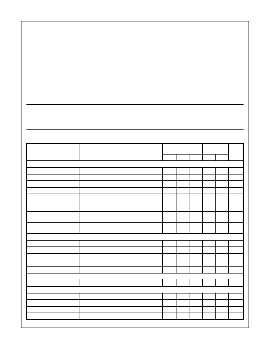
Electrical Specifications
V
DD
= V
CC
= V
AHB
= V
BHB
= 12V, V
SS
= V
ALS
= V
BLS
= V
AHS
= V
BHS
= 0V, R
HDEL
= R
LDEL
= 100K and
T
A
= 25
o
C, Unless Otherwise Specified
PARAMETER
SYMBOL
TEST CONDITIONS
T
J
= 25
o
C
T
JS
= -40
o
C
TO 125
o
C
UNITS
MIN
TYP
MAX
MIN
MAX
SUPPLY CURRENTS AND CHARGE PUMPS
V
DD
Quiescent Current
I
DD
All inputs = 0V
8.5
10.5
14.5
7.5
14.5
mA
V
DD
Operating Current
I
DDO
Outputs switching f = 500kHz
9.5
12.5
15.5
8.5
15.5
mA
V
CC
Quiescent Current
I
CC
All Inputs = 0V, I
ALO
= I
BLO
= 0
-
0.1
10
-
20
µ
A
V
CC
Operating Current
I
CCO
f = 500kHz, No Load
1
1.25
2.0
0.8
3
mA
AHB, BHB Quiescent Current -
Qpump Output Current
I
AHB
, I
BHB
All Inputs = 0V, I
AHO
= I
BHO
= 0
V
DD
= V
CC
= V
AHB
= V
BHB
= 10V
-50
-30
-11
-60
-10
µ
A
AHB, BHB Operating Current
I
AHBO
, I
BHBO
f = 500kHz, No Load
0.6
1.2
1.5
0.5
1.9
mA
AHS, BHS, AHB, BHB Leakage
Current
I
HLK
V
BHS
= V
AHS
= 80V,
V
AHB
= V
BHB
= 93V
-
0.02
1.0
-
10
µ
A
AHB-AHS, BHB-BHS Qpump
Output Voltage
V
AHB
-V
AHS
V
BHB
-V
BHS
I
AHB
= I
AHB
= 0, No Load
11.5
12.6
14.0
10.5
14.5
V
INPUT PINS: ALI, BLI, AHI, BHI, AND DIS
Low Level Input Voltage
V
IL
Full Operating Conditions
-
-
1.0
-
0.8
V
High Level Input Voltage
V
IH
Full Operating Conditions
2.5
-
-
2.7
-
V
Input Voltage Hysteresis
-
35
-
-
-
mV
Low Level Input Current
I
IL
V
IN
= 0V, Full Operating Conditions
-130
-100
-75
-135
-65
µ
A
High Level Input Current
I
IH
V
IN
= 5V, Full Operating Conditions
-1
-
+1
-10
+10
µ
A
TURN-ON DELAY PINS: LDEL AND HDEL
LDEL, HDEL Voltage
V
HDEL
, V
LDEL
I
HDEL
= I
LDEL
= -100
µ
A
4.9
5.1
5.3
4.8
5.4
V
GATE DRIVER OUTPUT PINS: ALO, BLO, AHO, AND BHO
Low Level Output Voltage
V
OL
I
OUT
= 100mA
0.7
0.85
1.0
0.5
1.1
V
High Level Output Voltage
V
CC
-V
OH
I
OUT
= -100mA
0.8
0.95
1.1
0.5
1.2
V
Peak Pullup Current
I
O
+
V
OUT
= 0V
1.7
2.6
3.8
1.4
4.1
A
Peak Pulldown Current
I
O
-
V
OUT
= 12V
1.7
2.4
3.3
1.3
3.6
A

4
HIP4081A
Undervoltage, Rising Threshold
UV+
8.1
8.8
9.4
8.0
9.5
V
Undervoltage, Falling Threshold
UV-
7.6
8.3
8.9
7.5
9.0
V
Undervoltage, Hysteresis
HYS
0.25
0.4
0.65
0.2
0.7
V
Switching Specifications
V
DD
= V
CC
= V
AHB
= V
BHB
= 12V, V
SS
= V
ALS
= V
BLS
= V
AHS
= V
BHS
= 0V, R
HDEL
= R
LDEL
= 10K,
C
L
= 1000pF.
PARAMETER
SYMBOL
TEST CONDITIONS
T
J
= 25
o
C
T
JS
= -40
o
C
TO 125
o
C
UNITS
MIN
TYP
MAX
MIN
MAX
Lower Turn-off Propagation Delay
(ALI-ALO, BLI-BLO)
T
LPHL
-
30
60
-
80
ns
Upper Turn-off Propagation Delay
(AHI-AHO, BHI-BHO)
T
HPHL
-
35
70
-
90
ns
Lower Turn-on Propagation Delay
(ALI-ALO, BLI-BLO)
T
LPLH
R
HDEL
= R
LDEL
= 10K
-
45
70
-
90
ns
Upper Turn-on Propagation Delay
(AHI-AHO, BHI-BHO)
T
HPLH
R
HDEL
= R
LDEL
= 10K
-
60
90
-
110
ns
Rise Time
T
R
-
10
25
-
35
ns
Fall Time
T
F
-
10
25
-
35
ns
Turn-on Input Pulse Width
T
PWIN-ON
R
HDEL
= R
LDEL
= 10K
50
-
-
50
-
ns
Turn-off Input Pulse Width
T
PWIN-OFF
R
HDEL
= R
LDEL
= 10K
40
-
-
40
-
ns
Turn-on Output Pulse Width
T
PWOUT-ON
R
HDEL
= R
LDEL
= 10K
40
-
-
40
-
ns
Turn-off Output Pulse Width
T
PWOUT-OFF
R
HDEL
= R
LDEL
= 10K
30
-
-
30
-
ns
Disable Turn-off Propagation Delay
(DIS - Lower Outputs)
T
DISLOW
-
45
75
-
95
ns
Disable Turn-off Propagation Delay
(DIS - Upper Outputs)
T
DISHIGH
-
55
85
-
105
ns
Disable to Lower Turn-on Propagation Delay
(DIS - ALO and BLO)
T
DLPLH
-
40
70
-
90
ns
Refresh Pulse Width (ALO and BLO)
T
REF-PW
240
410
550
200
600
ns
Disable to Upper Enable (DIS - AHO and BHO)
T
UEN
-
450
620
-
690
ns
TRUTH TABLE
INPUT
OUTPUT
ALI, BLI
AHI, BHI
U/V
DIS
ALO, BLO
AHO, BHO
X
X
X
1
0
0
1
X
0
0
1
0
0
1
0
0
0
1
0
0
0
0
0
0
X
X
1
X
0
0
NOTE:
X signifies that input can be either a "1" or "0".
Electrical Specifications
V
DD
= V
CC
= V
AHB
= V
BHB
= 12V, V
SS
= V
ALS
= V
BLS
= V
AHS
= V
BHS
= 0V, R
HDEL
= R
LDEL
= 100K and
T
A
= 25
o
C, Unless Otherwise Specified (Continued)
PARAMETER
SYMBOL
TEST CONDITIONS
T
J
= 25
o
C
T
JS
= -40
o
C
TO 125
o
C
UNITS
MIN
TYP
MAX
MIN
MAX
5
HIP4081A
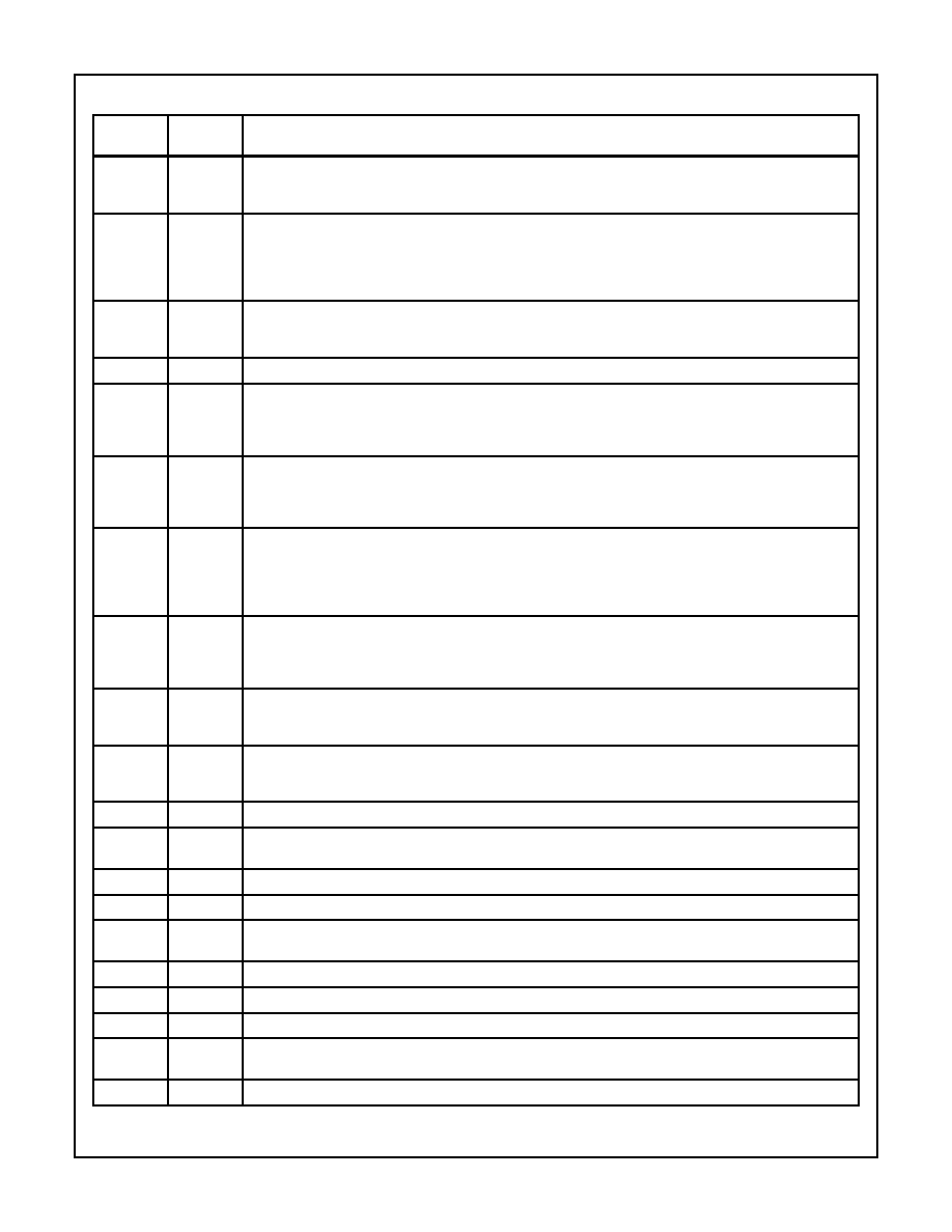
Pin Descriptions
PIN
NUMBER
SYMBOL
DESCRIPTION
1
BHB
B High-side Bootstrap supply. External bootstrap diode and capacitor are required. Connect cathode of boot-
strap diode and positive side of bootstrap capacitor to this pin. Internal charge pump supplies 30
µ
A out of this
pin to maintain bootstrap supply. Internal circuitry clamps the bootstrap supply to approximately 12.8V.
2
BHI
B High-side Input. Logic level input that controls BHO driver (Pin 20). BLI (Pin 5) high level input overrides BHI
high level input to prevent half-bridge shoot-through, see Truth Table. DIS (Pin 3) high level input overrides BHI
high level input. The pin can be driven by signal levels of 0V to 15V (no greater than V
DD
). An internal 100
µ
A
pull-up to V
DD
will hold BHI high, so no connection is required if high-side and low-side outputs are to be con-
trolled by the low-side input.
3
DIS
DISable input. Logic level input that when taken high sets all four outputs low. DIS high overrides all other inputs.
When DIS is taken low the outputs are controlled by the other inputs. The pin can be driven by signal levels of
0V to 15V (no greater than V
DD
). An internal 100
µ
A pull-up to V
DD
will hold DIS high if this pin is not driven.
4
V
SS
Chip negative supply, generally will be ground.
5
BLI
B Low-side Input. Logic level input that controls BLO driver (Pin 18). If BHI (Pin 2) is driven high or not connected
externally then BLI controls both BLO and BHO drivers, with dead time set by delay currents at HDEL and LDEL
(Pin 8 and 9). DIS (Pin 3) high level input overrides BLI high level input. The pin can be driven by signal levels
of 0V to 15V (no greater than V
DD
). An internal 100
µ
A pull-up to V
DD
will hold BLI high if this pin is not driven.
6
ALI
A Low-side Input. Logic level input that controls ALO driver (Pin 13). If AHI (Pin 7) is driven high or not connected
externally then ALI controls both ALO and AHO drivers, with dead time set by delay currents at HDEL and LDEL
(Pin 8 and 9). DIS (Pin 3) high level input overrides ALI high level input. The pin can be driven by signal levels
of 0V to 15V (no greater than V
DD
). An internal 100
µ
A pull-up to V
DD
will hold ALI high if this pin is not driven.
7
AHI
A High-side Input. Logic level input that controls AHO driver (Pin 11). ALI (Pin 6) high level input overrides AHI
high level input to prevent half-bridge shoot-through, see Truth Table. DIS (Pin 3) high level input overrides AHI
high level input. The pin can be driven by signal levels of 0V to 15V (no greater than V
DD
). An internal 100
µ
A
pull-up to V
DD
will hold AHI high, so no connection is required if high-side and low-side outputs are to be con-
trolled by the low-side input.
8
HDEL
High-side turn-on DELay. Connect resistor from this pin to V
SS
to set timing current that defines the turn-on de-
lay of both high-side drivers. The low-side drivers turn-off with no adjustable delay, so the HDEL resistor guar-
antees no shoot-through by delaying the turn-on of the high-side drivers. HDEL reference voltage is
approximately 5.1V.
9
LDEL
Low-side turn-on DELay. Connect resistor from this pin to V
SS
to set timing current that defines the turn-on delay
of both low-side drivers. The high-side drivers turn-off with no adjustable delay, so the LDEL resistor guarantees
no shoot-through by delaying the turn-on of the low-side drivers. LDEL reference voltage is approximately 5.1V.
10
AHB
A High-side Bootstrap supply. External bootstrap diode and capacitor are required. Connect cathode of boot-
strap diode and positive side of bootstrap capacitor to this pin. Internal charge pump supplies 30
µ
A out of this
pin to maintain bootstrap supply. Internal circuitry clamps the bootstrap supply to approximately 12.8V.
11
AHO
A High-side Output. Connect to gate of A High-side power MOSFET.
12
AHS
A High-side Source connection. Connect to source of A High-side power MOSFET. Connect negative side of
bootstrap capacitor to this pin.
13
ALO
A Low-side Output. Connect to gate of A Low-side power MOSFET.
14
ALS
A Low-side Source connection. Connect to source of A Low-side power MOSFET.
15
V
CC
Positive supply to gate drivers. Must be same potential as V
DD
(Pin 16). Connect to anodes of two bootstrap
diodes.
16
V
DD
Positive supply to lower gate drivers. Must be same potential as V
CC
(Pin 15). De-couple this pin to V
SS
(Pin 4).
17
BLS
B Low-side Source connection. Connect to source of B Low-side power MOSFET.
18
BLO
B Low-side Output. Connect to gate of B Low-side power MOSFET.
19
BHS
B High-side Source connection. Connect to source of B High-side power MOSFET. Connect negative side of
bootstrap capacitor to this pin.
20
BHO
B High-side Output. Connect to gate of B High-side power MOSFET.