1
®
CAUTION: These devices are sensitive to electrostatic discharge; follow proper IC Handling Procedures.
1-888-INTERSIL or 321-724-7143
|
Intersil (and design) is a registered trademark of Intersil Americas Inc.
Copyright © Intersil Americas Inc. 2004. All Rights Reserved.
All other trademarks mentioned are the property of their respective owners.
HIP2101
100V/2A Peak, Low Cost, High Frequency
Half Bridge Driver
The HIP2101 is a high frequency, 100V Half Bridge
N-Channel power MOSFET driver IC. It is equivalent to the
HIP2100 with the added advantage of full TTL/CMOS
compatible logic input pins. The low-side and high-side gate
drivers are independently controlled and matched to 13ns.
This gives users total control over dead-time for specific
power circuit topologies. Undervoltage protection on both
the low-side and high-side supplies force the outputs low. An
on-chip diode eliminates the discrete diode required with
other driver ICs. A new level-shifter topology yields the low-
power benefits of pulsed operation with the safety of DC
operation. Unlike some competitors, the high-side output
returns to its correct state after a momentary undervoltage of
the high-side supply.
Features
· Drives N-Channel MOSFET Half Bridge
· SOIC, EPSOIC, QFN and DFN Package Options
· SOIC, EPSOIC and DFN Packages Compliant with 100V
Conductor Spacing Guidelines of IPC-2221
· Pb-free Product Available
(RoHS Compliant)
· Bootstrap Supply Max Voltage to 114VDC
· On-Chip 1
Bootstrap Diode
· Fast Propagation Times for Multi-MHz Circuits
· Drives 1000pF Load with Rise and Fall Times Typ. 10ns
· TTL/CMOS Input Thresholds Increase Flexibility
· Independent Inputs for Non-Half Bridge Topologies
· No Start-Up Problems
· Outputs Unaffected by Supply Glitches, HS Ringing Below
Ground, or HS Slewing at High dv/dt
· Low Power Consumption
· Wide Supply Range
· Supply Undervoltage Protection
· 3
Output Driver Resistance
· QFN/DFN Package:
- Compliant to JEDEC PUB95 MO-220
QFN - Quad Flat No Leads - Package Outline
- Near Chip Scale Package footprint, which improves
PCB efficiency and has a thinner profile
Applications
· Telecom Half Bridge Power Supplies
· Avionics DC-DC Converters
· Two-Switch Forward Converters
· Active Clamp Forward Converters
Ordering Information
PART NUMBER
TEMP.
RANGE (°C)
PACKAGE
PKG.
DWG. #
HIP2101IB
-40 to 125
8 Ld SOIC
M8.15
HIP2101IBZ (Note 1)
-40 to 125
8 Ld SOIC (Pb-free) M8.15
HIP2101EIB
-40 to 125
8 Ld EPSOIC
M8.15C
HIP2101EIBZ
(Note 1)
-40 to 125
8 Ld EPSOIC
(Pb-free)
M8.15C
HIP2101IR
-40 to 125
16 Ld 5x5 QFN
L16.5x5
HIP2101IRZ (Note 1)
-40 to 125
16 Ld 5x5 QFN
(Pb-free)
L16.5x5
HIP2101IR4
-40 to 125
12 Ld 4x4 DFN
L12.4x4A
HIP2101IR4Z
(Note 1)
-40 to 125
12 Ld 4x4 DFN
(Pb-free)
L12.4x4A
NOTES:
1.
Intersil Pb-free products employ special Pb-free material sets;
molding compounds/die attach materials and 100% matte tin
plate termination finish, which are RoHS compliant and
compatible with both SnPb and Pb-free soldering operations.
Intersil Pb-free products are MSL classified at Pb-free peak reflow
temperatures that meet or exceed the Pb-free requirements of
IPC/JEDEC J STD-020C.
2. Add "T" suffix for Tape and Reel packing option.
Data Sheet
October 21, 2004
FN9025.8
2
FN9025.8
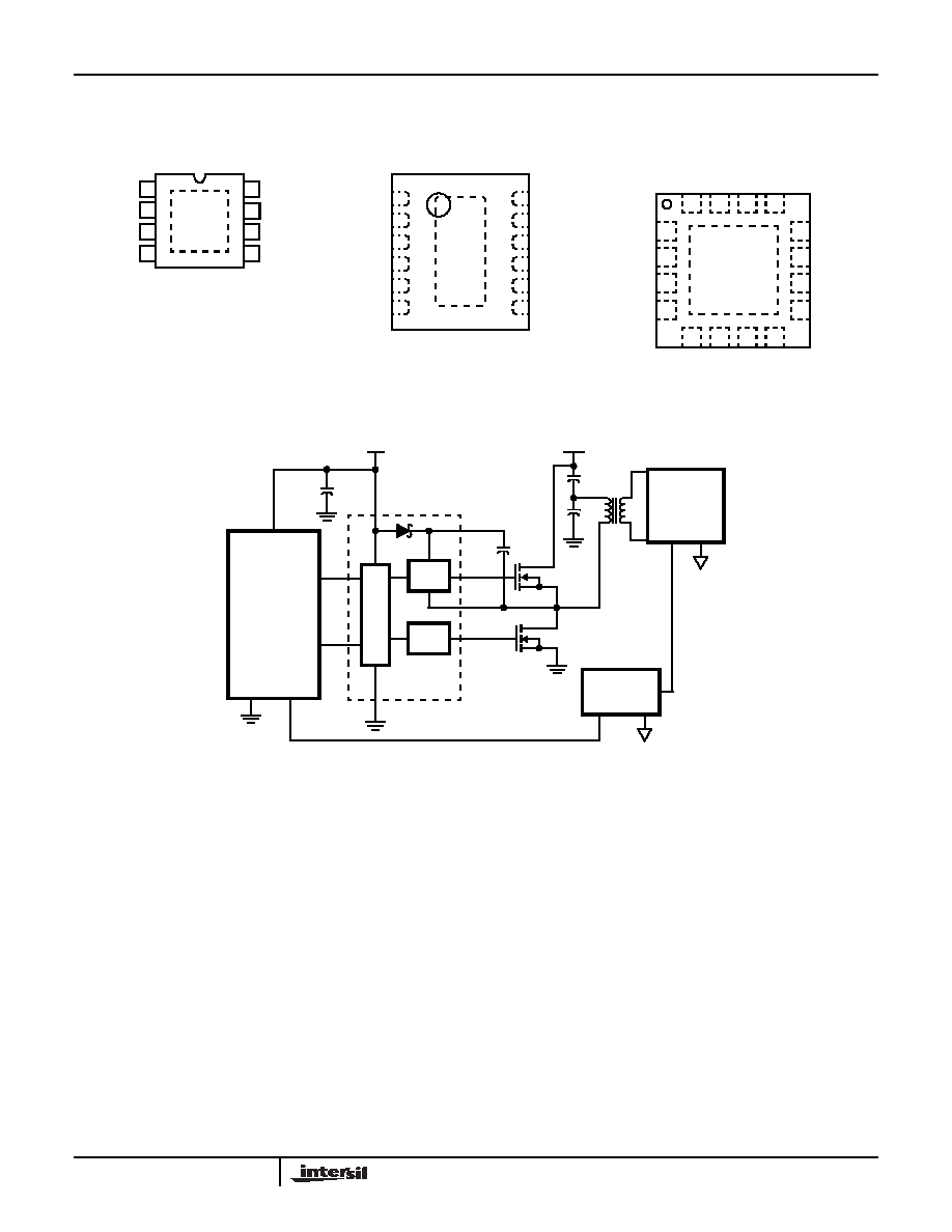
Application Block Diagram
Pinouts
HIP2101 (SOIC, EPSOIC)
TOP VIEW
HIP2101IR4 (DFN)
TOP VIEW
HIP2101 (QFN)
TOP VIEW
NOTE: EPAD = Exposed PAD.
5
6
8
7
4
3
2
1
V
DD
HB
HO
HS
LO
LI
HI
V
SS
EPAD
V
DD
NC
NC
HB
HO
LO
V
SS
NC
NC
LI
HS
HI
2
3
4
1
5
11
10
9
12
8
6
7
EPAD
1
3
4
15
HB
HO
V
DD
LO
16
14
13
2
12
10
9
11
6
5
7
8
V
SS
LI
HS
HI
NC
NC
NC
NC
NC
NC
NC
NC
EPAD
SECONDARY
CIRCUIT
+100V
CO
N
T
RO
L
CONTROLLER
PWM
LI
HI
HO
LO
V
DD
HS
HB
+12V
V
SS
HIP2101
REFERENCE
AND
ISOLATION
DRIVE
LO
DRIVE
HI
HIP2101
3
FN9025.8
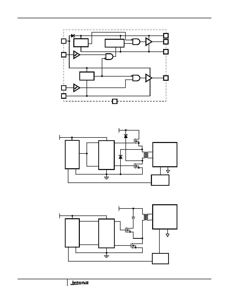
Functional Block Diagram
UNDER
VOLTAGE
V
DD
HI
LI
V
SS
DRIVER
DRIVER
HB
HO
HS
LO
LEVEL SHIFT
UNDER
VOLTAGE
EPAD (EPSOIC, QFN and DFN PACKAGES ONLY)
*EPAD = Exposed Pad. The EPAD is electrically isolated from all other pins. For
best thermal performance connect the EPAD to the PCB power ground plane.
SECONDARY
HIP
2101
ISOLATION
PWM
+48V
+12V
CIRCUIT
FIGURE 1. TWO-SWITCH FORWARD CONVERTER
SECONDARY
CIRCUIT
HIP
2101
ISOLATION
PWM
+48V
+12V
FIGURE 2. FORWARD CONVERTER WITH AN ACTIVE CLAMP
HIP2101
4
FN9025.8
Absolute Maximum Ratings
Thermal Information
Supply Voltage, V
DD,
V
HB
-V
HS
(Notes 3, 4) . . . . . . . . -0.3V to 18V
LI and HI Voltages (Note 4) . . . . . . . . . . . . . . . . . . . . . -0.3V to 7.0V
Voltage on LO (Note 4) . . . . . . . . . . . . . . . . . . . -0.3V to V
DD
+0.3V
Voltage on HO (Note 4) . . . . . . . . . . . . . . . V
HS
-0.3V to V
HB
+0.3V
Voltage on HS (Continuous) (Note 4) . . . . . . . . . . . . . . -1V to 110V
Voltage on HB (Note 4) . . . . . . . . . . . . . . . . . . . . . . . . . . . . . +118V
Average Current in V
DD
to HB diode. . . . . . . . . . . . . . . . . . . 100mA
ESD Classification . . . . . . . . . . . . . . . . . . . . . . . . . . . Class 1 (1kV)
Maximum Recommended Operating Conditions
Supply Voltage, V
DD
. . . . . . . . . . . . . . . . . . . . . . . . +9V to 14.0VDC
Voltage on HS . . . . . . . . . . . . . . . . . . . . . . . . . . . . . . . . -1V to 100V
Voltage on HS . . . . . . . . . . . . . . .(Repetitive Transient) -5V to 105V
Voltage on HB . . V
HS
+8V to V
HS
+14.0V and V
DD
-1V to V
DD
+100V
HS Slew Rate. . . . . . . . . . . . . . . . . . . . . . . . . . . . . . . . . . . . <50V/ns
Thermal Resistance (Typical)
JA
(°C/W)
JC
(°C/W)
SOIC (Note 5) . . . . . . . . . . . . . . . . . . .
95
N/A
EPSOIC (Note 6) . . . . . . . . . . . . . . . . .
40
3.0
QFN (Note 6) . . . . . . . . . . . . . . . . . . . .
37
6.5
DFN (Note 6) . . . . . . . . . . . . . . . . . . . .
40
3.0
Max Power Dissipation at 25
o
C in Free Air (SOIC, Note 5) . . . . 1.3W
Max Power Dissipation at 25
o
C in Free Air (EPSOIC, Note 6). . 3.1W
Max Power Dissipation at 25
o
C in Free Air (QFN, Note 6). . . . . 3.3W
Storage Temperature Range . . . . . . . . . . . . . . . . . . . -65°C to 150°C
Junction Temperature Range . . . . . . . . . . . . . . . . . . -55°C to 150°C
Lead Temperature (Soldering 10s - SOIC Lead Tips Only). . 300°C
For Recommended soldering conditions see Tech Brief TB389.
CAUTION: Stresses above those listed in "Absolute Maximum Ratings" may cause permanent damage to the device. This is a stress only rating and operation of the
device at these or any other conditions above those indicated in the recommended operating conditions of this specification is not implied.
NOTES:
3. The HIP2101 is capable of derated operation at supply voltages exceeding 14V. Figure 16 shows the high-side voltage derating curve for this
mode of operation.
4. All voltages referenced to V
SS
unless otherwise specified.
5.
JA
is measured with the component mounted on a high effective thermal conductivity test board in free air. See Tech Brief TB379 for details.
6.
JA
is measured in free air with the component mounted on a high effective thermal conductivity test board with "direct attach" features.
JC,
the
"case temp" is measured at the center of the exposed metal pad on the package underside. See Tech Brief TB379.
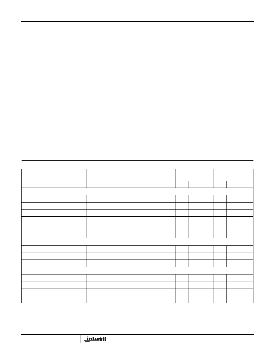
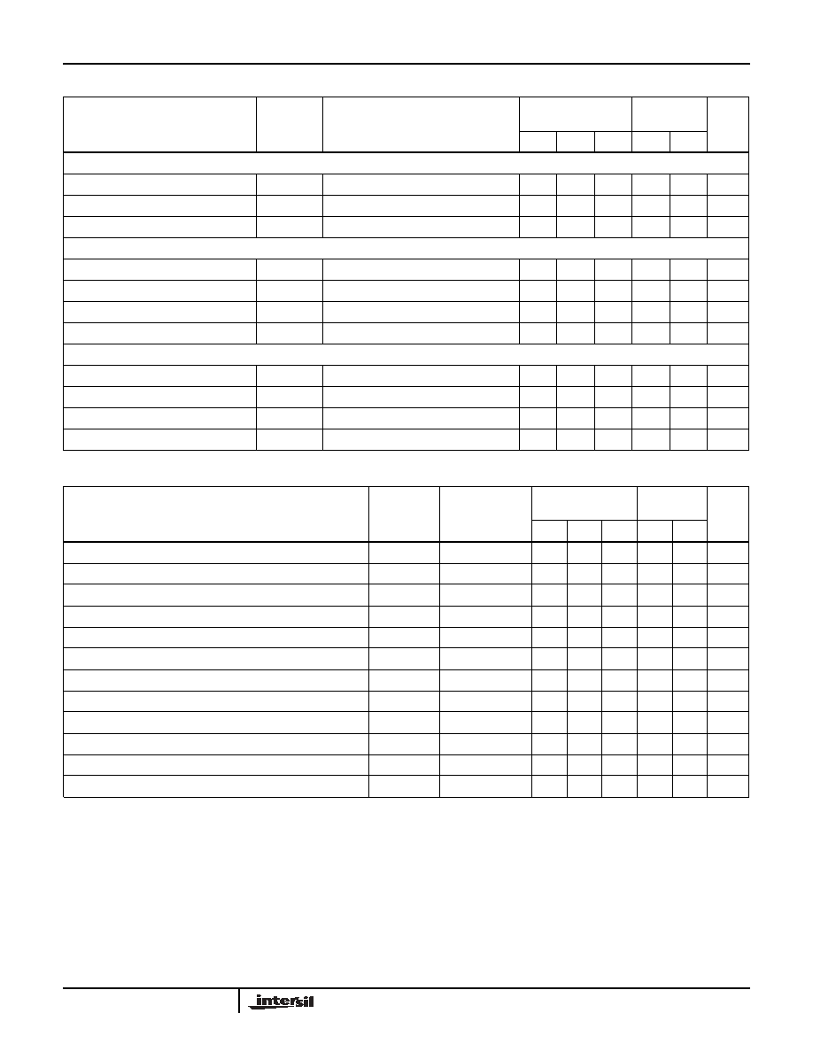
Electrical Specifications
V
DD
= V
HB
= 12V, V
SS
= V
HS
= 0V, No Load on LO or HO, Unless Otherwise Specified
PARAMETERS
SYMBOL
TEST CONDITIONS
T
J
= 25°C
T
J
= -40°C TO
125°C
UNITS
MIN
TYP
MAX
MIN
MAX
SUPPLY CURRENTS
V
DD
Quiescent Current
I
DD
LI = HI = 0V
-
0.3
0.45
-
0.6
mA
V
DD
Operating Current
I
DDO
f = 500kHz
-
1.7
3.0
-
3.4
mA
Total HB Quiescent Current
I
HB
LI = HI = 0V
-
0.1
0.15
-
0.2
mA
Total HB Operating Current
I
HBO
f = 500kHz
-
1.5
2.5
-
3
mA
HB to V
SS
Current, Quiescent
I
HBS
V
HS
= V
HB
= 114V
-
0.05
1.5
-
10
µ
A
HB to V
SS
Current, Operating
I
HBSO
f = 500kHz
-
0.7
-
-
-
mA
INPUT PINS
Low Level Input Voltage Threshold
V
IL
0.8
1.65
-
0.8
-
V
High Level Input Voltage Threshold
V
IH
-
1.65
2.2
-
2.2
V
Input Pulldown Resistance
R
I
-
200
-
100
500
k
UNDER VOLTAGE PROTECTION
V
DD
Rising Threshold
V
DDR
7
7.3
7.8
6.5
8
V
V
DD
Threshold Hysteresis
V
DDH
-
0.5
-
-
-
V
HB Rising Threshold
V
HBR
6.5
6.9
7.5
6
8
V
HB Threshold Hysteresis
V
HBH
-
0.4
-
-
-
V
HIP2101
5
FN9025.8
BOOT STRAP DIODE
Low-Current Forward Voltage
V
DL
I
VDD-HB
= 100
µ
A
-
0.45
0.70
-
0.7
V
High-Current Forward Voltage
V
DH
I
VDD-HB
= 100mA
-
0.7
0.92
-
1
V
Dynamic Resistance
R
D
I
VDD-HB
= 100mA
-
0.8
1
-
1.5
LO GATE DRIVER
Low Level Output Voltage
V
OLL
I
LO
= 100mA
-
0.25
0.3
-
0.4
V
High Level Output Voltage
V
OHL
I
LO
= -100mA, V
OHL
= V
DD
-V
LO
-
0.25
0.3
-
0.4
V
Peak Pullup Current
I
OHL
V
LO
= 0V
-
2
-
-
-
A
Peak Pulldown Current
I
OLL
V
LO
= 12V
-
2
-
-
-
A
HO GATE DRIVER
Low Level Output Voltage
V
OLH
I
HO
= 100mA
-
0.25
0.3
-
0.4
V
High Level Output Voltage
V
OHH
I
HO
= -100mA, V
OHH
= V
HB
-V
HO
-
0.25
0.3
-
0.4
V
Peak Pullup Current
I
OHH
V
HO
= 0V
-
2
-
-
-
A
Peak Pulldown Current
I
OLH
V
HO
= 12V
-
2
-
-
-
A
Electrical Specifications
V
DD
= V
HB
= 12V, V
SS
= V
HS
= 0V, No Load on LO or HO, Unless Otherwise Specified (Continued)
PARAMETERS
SYMBOL
TEST CONDITIONS
T
J
= 25°C
T
J
= -40°C TO
125°C
UNITS
MIN
TYP
MAX
MIN
MAX
Switching Specifications
V
DD
= V
HB
= 12V, V
SS
= V
HS
= 0V, No Load on LO or HO, Unless Otherwise Specified
PARAMETERS
SYMBOL
TEST
CONDITIONS
T
J
= 25°C
T
J
= -40°C
TO 125°C
UNITS
MIN
TYP
MAX
MIN
MAX
Lower Turn-Off Propagation Delay (LI Falling to LO Falling)
t
LPHL
-
25
43
-
56
ns
Upper Turn-Off Propagation Delay (HI Falling to HO Falling)
t
HPHL
-
25
43
-
56
ns
Lower Turn-On Propagation Delay (LI Rising to LO Rising)
t
LPLH
-
25
43
-
56
ns
Upper Turn-On Propagation Delay (HI Rising to HO Rising)
t
HPLH
-
25
43
-
56
ns
Delay Matching: Lower Turn-On and Upper Turn-Off
t
MON
-
2
13
-
16
ns
Delay Matching: Lower Turn-Off and Upper Turn-On
t
MOFF
-
2
13
-
16
ns
Either Output Rise/Fall Time
t
RC,
t
FC
C
L
= 1000pF
-
10
-
-
-
ns
Either Output Rise/Fall Time (3V to 9V)
t
R,
t
F
C
L
= 0.1
µ
F
-
0.5
0.6
-
0.8
us
Either Output Rise Time Driving DMOS
t
RD
C
L
= IRFR120
-
20
-
-
-
ns
Either Output Fall Time Driving DMOS
t
FD
C
L
= IRFR120
-
10
-
-
-
ns
Minimum Input Pulse Width that Changes the Output
t
PW
-
-
-
-
50
ns
Bootstrap Diode Turn-On or Turn-Off Time
t
BS
-
10
-
-
-
ns
HIP2101